Supercharge Your Innovation With Domain-Expert AI Agents!

FFS type TFT-LCD array substrate structure and manufacture method thereof

An array substrate structure and manufacturing method technology, applied in semiconductor/solid-state device manufacturing, optics, instruments, etc., can solve the problems of uneven liquid crystal orientation and confusion of pixel electrodes, improve picture quality, eliminate step end difference, and improve freedom degree of effect

Active Publication Date: 2009-10-14
BOE TECH GRP CO LTD +1
View PDF0 Cites 35 Cited by
  • Summary
  • Abstract
  • Description
  • Claims
  • Application Information

AI Technical Summary

Problems solved by technology

[0005] The purpose of the present invention is to provide an FFS type TFT-LCD array substrate structure and its manufacturing method, which can effectively solve the technical defects of the array substrate structure in the prior art, such as disordered liquid crystal orientation caused by uneven pixel electrodes.

Method used


Image

  • FFS type TFT-LCD array substrate structure and manufacture method thereof
  • FFS type TFT-LCD array substrate structure and manufacture method thereof
  • FFS type TFT-LCD array substrate structure and manufacture method thereof

Examples


Embodiment Construction

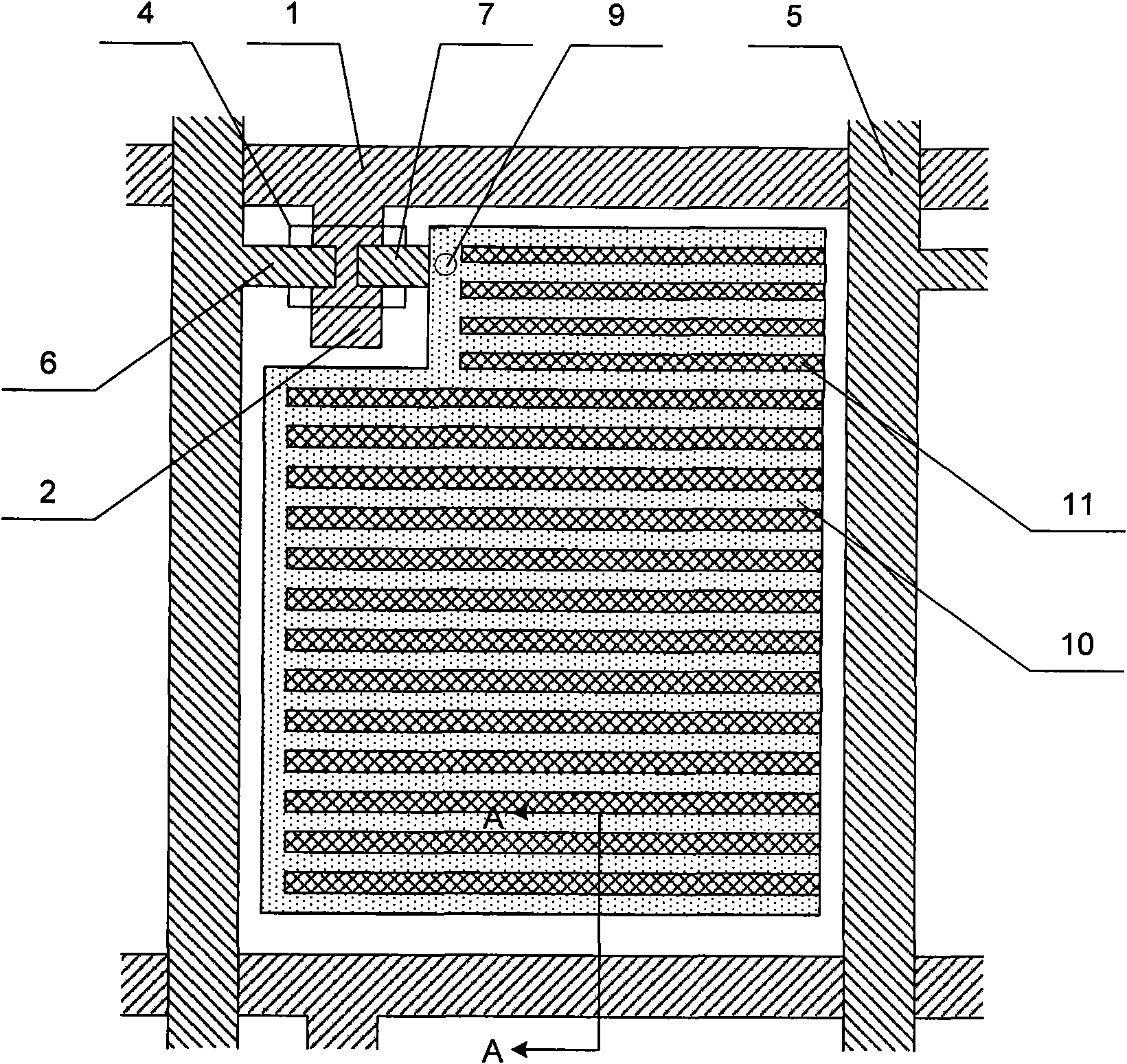
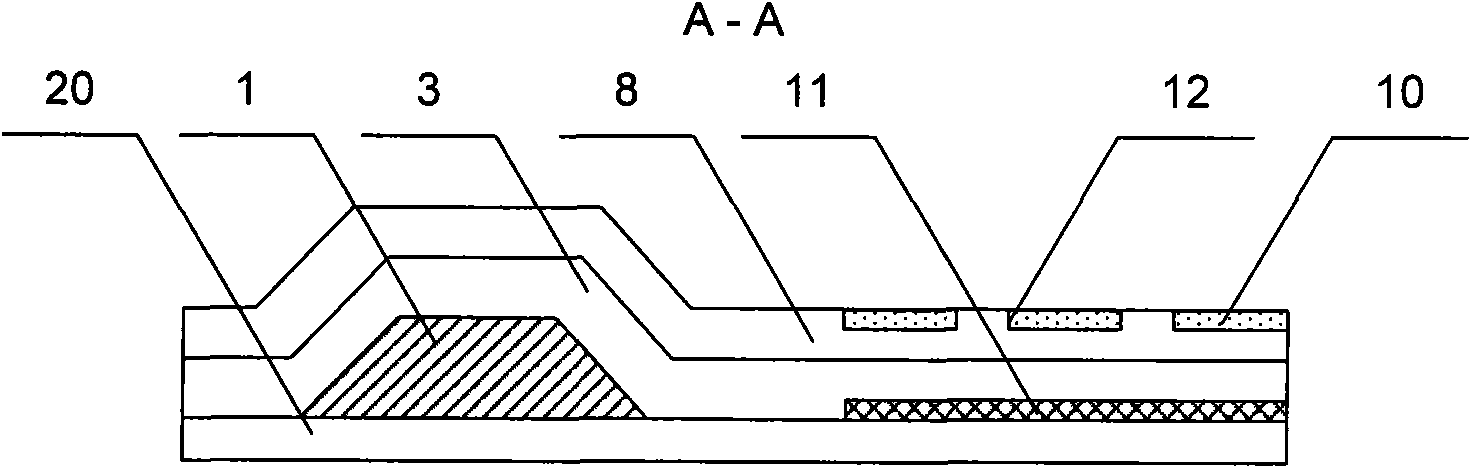
[0048] figure 1 It is a schematic diagram of the structure of the FFS type TFT-LCD array substrate of the present invention, figure 2 for figure 1 Middle A-A sectional view. Such as figure 1 , figure 2As shown, the array substrate structure of the present invention includes a substrate 20, on which gate lines 1, gate electrodes 2 and common electrodes 11 are formed, gate lines 1 and common electrodes 11 are arranged in isolation, and a gate insulating layer 3 is formed on the substrate and covers the gate lines 1. The gate electrode 2 and the common electrode 11. The active layer 4 is formed on the gate insulating layer 3 and located on the gate electrode 2. The data line 5 is formed on the gate insulating layer 3 and is perpendicular to the gate line 1. The source The electrode 6 and the drain electrode 7 are formed on the active layer 4 to form a TFT channel, the passivation layer 8 is formed on the entire substrate, and strip-shaped passivation layer grooves 12 arr...


PUM


Abstract

The invention relates to an FFS type TFT-LCD array substrate structure and a manufacture method thereof. The array substrate structure comprises a substrate, a public electrode, a grid line, a grid electrode, a grid insulating layer, an active layer, a data wire, a source electrode, a drain electrode and a passivation layer, wherein the public electrode, the grid line, the grid electrode, the grid insulating layer, the data wire, the source electrode, the drain electrode and the passivation layer are formed on the substrate; and the active layer is formed on the grid insulating layer and positioned on the grid electrode. Passivation layer grooves which are in strip shapes and are sequentially arranged are formed in a pixel area; a passivation layer through hole is formed at the position of the drain electrode; pixel electrodes are formed on the passivation layer, positioned in the passivation layer grooves and connected with the drain electrode through the passivation layer through hole. The invention farthest eliminates the terminal temperature difference (TTD) of the pixel electrodes in the pixel area, and flat surfaces of the pixel electrodes ensure that the subsequent friction orientation process of orientation films can obtain uniform orientation angles, thereby the quality of pictures is improved, and the degree of freedom for designing the pixel electrodes is greatly improved.

Description

technical field [0001] The invention relates to a thin film transistor liquid crystal display and a manufacturing method thereof, in particular to an FFS type TFT-LCD array substrate structure and a manufacturing method thereof. Background technique [0002] In recent years, with the popularization of digital TV, the traditional CRT display has been gradually replaced by a new generation of display devices, including PDP, OLED, LCD, etc., among which Thin Film Transistor Liquid Crystal Display (TFT-LCD for short) ) has the characteristics of small size, low power consumption, no radiation, and high display resolution, and has begun to be widely popularized and become a mainstream product. Fringe Field Switching (FFS for short) is one of the technologies that have appeared in recent years to improve the image quality of LCDs, and can simultaneously meet the requirements of high penetration and large viewing angles. The so-called FFS technology uses the fringe electric field ...

Claims


Application Information

Patent Timeline
Patent Type & Authority Applications(China)
IPC IPC(8): G02F1/1362H01L27/12H01L23/522H01L21/84H01L21/768
Inventor 陈旭闵泰烨林承武谢振宇
Owner BOE TECH GRP CO LTD
Features
  • R&D
  • Intellectual Property
  • Life Sciences
  • Materials
  • Tech Scout
  • Unparalleled Data Quality
  • Higher Quality Content
  • 60% Fewer Hallucinations
Learn More