Wafer alignment mark
A technology for aligning marks and wafers, applied in electrical components, electrical solid-state devices, circuits, etc., can solve problems such as defects or stress, affecting the quality and yield of semiconductor devices, and achieve the effect of improving yield
- Summary
- Abstract
- Description
- Claims
- Application Information
AI Technical Summary
Benefits of technology
Problems solved by technology
Method used
Image

Examples
Embodiment Construction
[0015] The wafer alignment mark of the present invention will be described in further detail below.
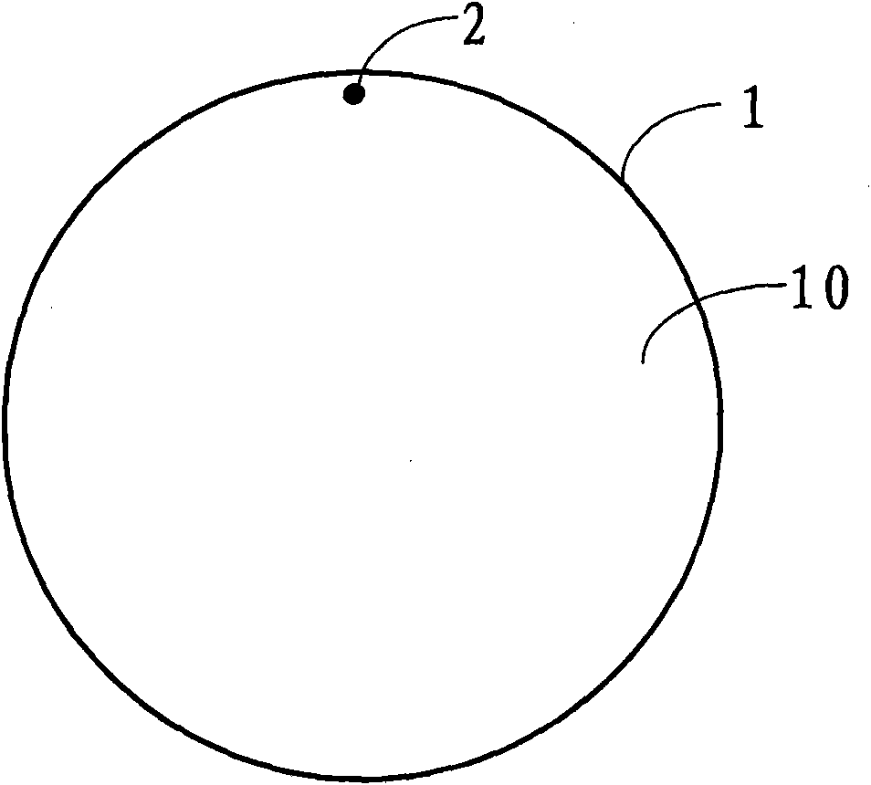
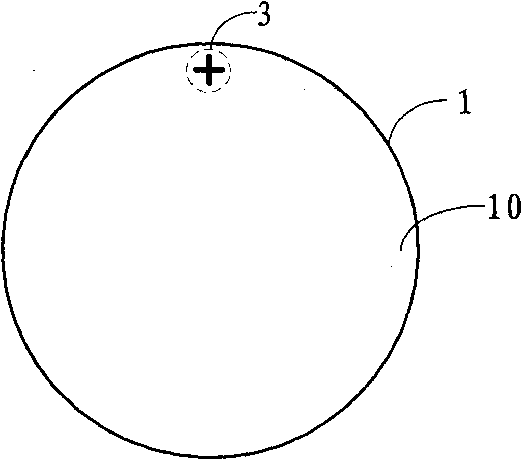
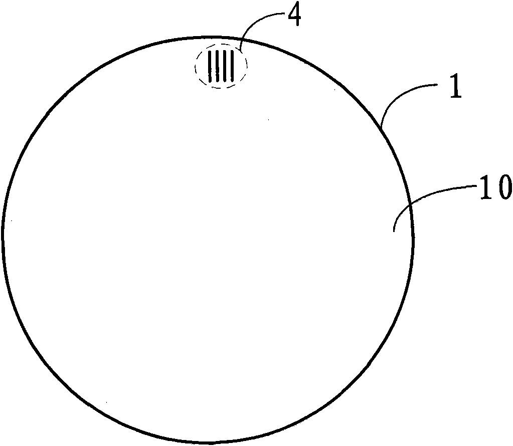
[0016] The wafer alignment mark of the present invention is disposed on the edge of the back surface 10 of the wafer 1 , and the wafer alignment mark is an axis-symmetric laser mark.
[0017] It should be noted that the surface opposite to the back surface 10 of the wafer 1 , that is, the front surface of the wafer 1 is used to manufacture semiconductor devices.
[0018] see figure 1 , In the first embodiment of the present invention, the wafer alignment mark 2 is disposed on the back surface 10 of the wafer 1, which is a laser mark and is a circle, and the diameter of the circle is 10 microns.
[0019] see figure 2 , In the second embodiment of the present invention, the wafer alignment mark 3 is disposed on the back surface 10 of the wafer 1 , which is a laser marking and is a cross.
[0020] see image 3 , in the third embodiment of the present invention, the wafer ali...
PUM
 Abstract
Description
Claims
Application Information