Solar silicon chip detecting machine platform and detecting method

A detection method and silicon chip technology, applied in semiconductor/solid-state device testing/measurement, sustainable manufacturing/processing, electrical components, etc., can solve the problems of increased detection, vulnerability, high angular acceleration, etc.

Inactive Publication Date: 2009-10-28
CHROMA ELECTRONICS SHENZHEN
View PDF0 Cites 36 Cited by
  • Summary
  • Abstract
  • Description
  • Claims
  • Application Information

AI Technical Summary

Problems solved by technology

During the continuous turning process, there is a stress concentration effect at the lower end along the direction of gravity, and a slightly faster speed may cause edge damage or micro-crakes. The former can still be detected visually, while the latter increases the trouble of detection
[0006] The design of the double-turned waterwheel, the radius is too small, the angular acceleration in the direction related to gravity is high and easy to be damaged; the radius is too large, it will occupy a huge space
Even if efforts are made to reduce the radius, it takes at least three times the space for placing solar silicon chips and two times the running space for turning the water wheel in the direction of the process, and the overall size of the machine cannot be reduced.

Method used


Image

  • Solar silicon chip detecting machine platform and detecting method
  • Solar silicon chip detecting machine platform and detecting method
  • Solar silicon chip detecting machine platform and detecting method

Examples


Embodiment Construction

[0036] The present invention will be further elaborated below in conjunction with the accompanying drawings and specific embodiments. These examples should be understood as only for illustrating the present invention but not for limiting the protection scope of the present invention. After reading the contents of the present invention, those skilled in the art can make various changes or modifications to the present invention, and these equivalent changes and modifications also fall within the scope defined by the appended claims of the present invention.

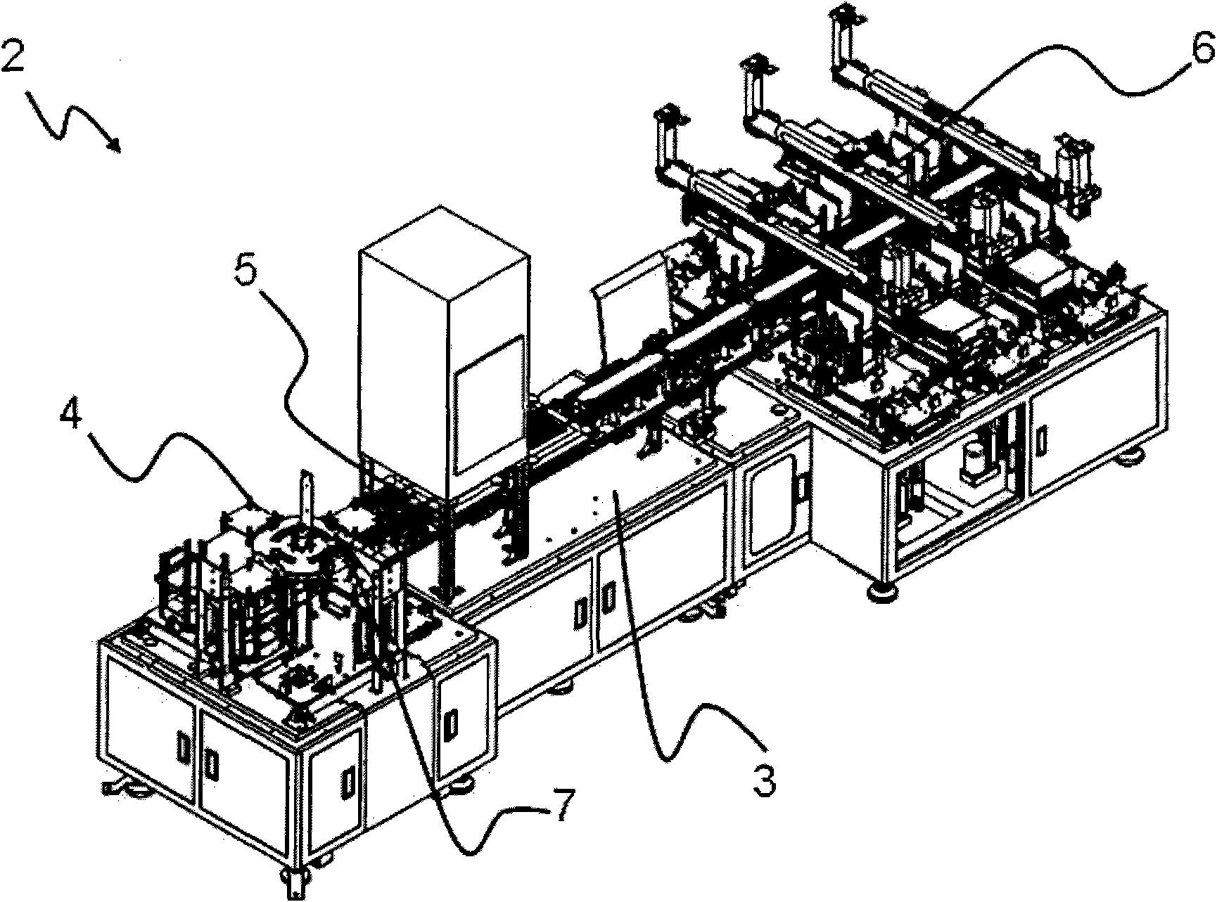
[0037] Such as image 3 As shown, the solar silicon chip detection machine 2 provided by the first preferred embodiment of the present invention includes a base 3, a suction feeding device 4, a load detection device 5, a suction classification device 6, a second surface detection device 7 and a processing device .

[0038] Such as Figure 4 and Figure 5 As shown, the second surface detection device 7 is set correspondi...


PUM


Abstract

The invention discloses a solar silicon chip detecting machine platform for detecting solar silicon chips one by one. All silicon chips to be detected have first surfaces and second surfaces which are mutually opposite and are respectively provided with electrodes. The detecting machine platform comprises a base; an absorbing feeding device is arranged on the base and absorbs the silicon chips to be detected from the first surfaces; a bearing detecting device is arranged on the base for bearing the second surfaces of the silicon chips to be detected from the absorbing feeding device to move and detect the characteristics of the first surfaces of the silicon chips to be detected along a radial direction; an absorbing sorting device is assembled on the base and absorbs the silicon chips to be detected from the bearing detecting device from the first surfaces; a second surface detecting device is arranged on the base, and corresponds to one of the absorbing feeding device or the absorbing sorting device; and a processing device is used for receiving information from the bearing detecting device and the second surface detecting device and commanding the absorbing sorting device. In addition, the invention also discloses a solar silicon chip detecting method.

Description

technical field [0001] The invention relates to a solar silicon chip detection machine; the invention also relates to a solar silicon chip detection method. Background technique [0002] Mineral resources such as crude oil are becoming increasingly depleted, and the refining process is constantly polluted; while natural resources such as solar energy have the advantages of being inexhaustible, inexhaustible and free from environmental problems, they have become the key to the next generation of energy. Solar panels can Photoelectric conversion, converting the received light energy into electrical energy for utilization, is one of the better solutions for alternative energy. [0003] The main components that make up a solar panel are solar silicon chips, such as figure 1 As shown, the left side of the figure is the light-receiving surface of the solar silicon chip 1 , hereinafter referred to as the first surface 12 , and the right side is the non-light-receiving surface of t...

Claims


Application Information

Patent Timeline
Patent Type & Authority Applications(China)
IPC IPC(8): H01L31/18H01L21/66
CPCY02P70/50
Inventor 林汉声
Owner CHROMA ELECTRONICS SHENZHEN
Why Eureka
Try Eureka