Manufacturing method of light source module, optical plate, and master mould and sub-mould of the optical plate

A technology for light source modules and optical plates, which is applied in the field of manufacturing light source modules, optical plates, optical plates and their master molds and sub-moulds, and can solve the problems that the optical effect of the optical plate cannot be further improved, microstructures cannot be formed, and deformation, etc. , to achieve the effect of good light extraction efficiency, not easy to scratch, and avoid scratching

Inactive Publication Date: 2009-11-04
AU OPTRONICS CORP
View PDF0 Cites 21 Cited by
  • Summary
  • Abstract
  • Description
  • Claims
  • Application Information

AI Technical Summary

Problems solved by technology

However, if the plurality of microstructures 210 of the optical plate 200' are too close to each other so as to overlap, then as Figure 2B As shown, at this time, the diamond indenter D will not be able to form a normal microstructure 210, but a deformed microstructure 210′
It can be seen that the indentation processing method in the known technology cannot produce tightly packed microstructures, so the optical effect of the optical plate will also be limited and cannot be further improved

Method used


Image

  • Manufacturing method of light source module, optical plate, and master mould and sub-mould of the optical plate
  • Manufacturing method of light source module, optical plate, and master mould and sub-mould of the optical plate
  • Manufacturing method of light source module, optical plate, and master mould and sub-mould of the optical plate

Examples


Embodiment Construction

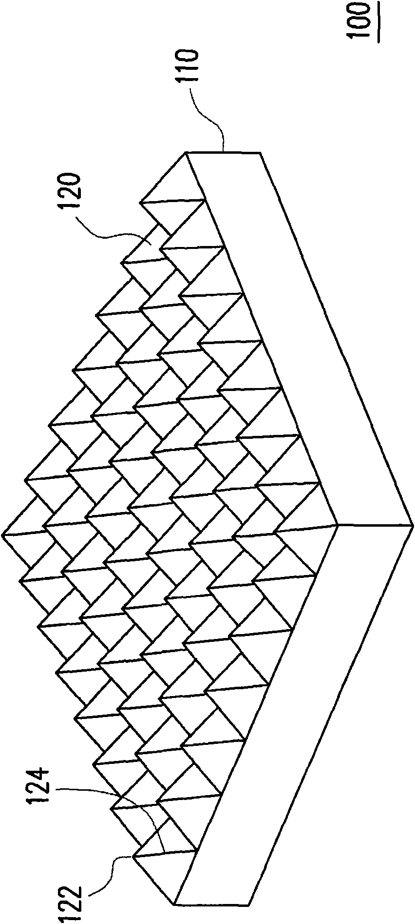
[0080] Optical board and light source module

[0081] image 3 It is a schematic diagram of a light source module 400 in a preferred embodiment of the present invention. Figure 4 is a schematic top view of the optical plate 300 . Figure 5 for correspondence Figure 4 The side views of the optical plate 300 of A-A', B-B' and C-C' are schematic.

[0082] Please also refer to image 3 , Figure 4 and Figure 5 , the light source module 400 includes an optical plate 300 and a light source 410 . The optical plate 300 includes a substrate 302 , a plurality of first protruding microstructures 312 , a plurality of second protruding microstructures 322 and a plurality of third protruding microstructures 332 . The substrate 302 has a first region 310 , a second region 320 , a third region 330 and a light incident region 302 b. In detail, the first area 310 is closest to the light incident area 302 b , the third area 330 is farthest from the light incident area 302 b , and the ...


PUM

PropertyMeasurementUnit
thicknessaaaaaaaaaa
thicknessaaaaaaaaaa
thicknessaaaaaaaaaa

Abstract

The invention discloses a manufacturing method of a light source module, an optical plate, and a master mould and a sub-mould of the optical plate. The optical plate comprises a substrate, a plurality of first microstructures, a plurality of second microstructures and a plurality of third microstructures. The substrate has a first area, a second area and a third area, and the second area is between the first area and the third area. A plurality of the first microstructures are arranged on a surface of the substrate in the first area at a predetermined spacing. A plurality of the second microstructures are arranged on the surface of the substrate in the second area. A plurality of the second microstructures have paired mutual connection at least, and a connection and the surface of the substrate are coplanar. A plurality of the third microstructures are arranged on the surface of the substrate in the third area, and a plurality of the third microstructures have paired partial superposition at least; wherein, the first microstructures, the second microstructures and the third microstructures have circular arc-shaped tips respectively. The method can help prevent moire generation, provide uniform and concentrated beams and be used for manufacturing a concaved microstructure mould and a convex microstructure mould with circular arc-shaped tips, and the optical plate with high light extraction efficiency.

Description

technical field [0001] The present invention relates to a light source module, a manufacturing method of a master mold and a sub-mould of an optical plate, an optical plate and a manufacturing method thereof, and in particular to a light source module with uniform and concentrated light, and an optical plate with an arc-shaped tip microstructure A method for manufacturing a master mold and a daughter mold, and an optical plate with good light extraction rate and a method for manufacturing the same. Background technique [0002] In liquid crystal displays, cold cathode fluorescent tubes (Cold Cathode Fluorescent Tube, CCFT) or light emitting diodes (Light Emitting Diode, LED) are generally used as light sources, and then the light emitted by the light sources is guided to the display screen through the light guide plate. In order to prevent the brightness unevenness of the liquid crystal display, it is necessary to use an optical plate to make the brightness of the entire scr...

Claims


Application Information

Patent Timeline
Patent Type & Authority Applications(China)
IPC IPC(8): F21S2/00F21V8/00G02F1/13357F21K9/60G02F1/1335
Inventor 潘昆志曾兆弘朱志宏田书豪陈轩德
Owner AU OPTRONICS CORP
Why Eureka
Try Eureka