Connection point structure as well as forming method and connecting structure thereof
A joint structure and contact technology, applied in the direction of electrical components, electrical solid devices, circuits, etc., can solve problems such as stress concentration, metal layer rupture, affecting electrical reliability, etc., and achieve the effect of avoiding stress concentration
- Summary
- Abstract
- Description
- Claims
- Application Information
AI Technical Summary
Problems solved by technology
Method used
Image

Examples
Embodiment
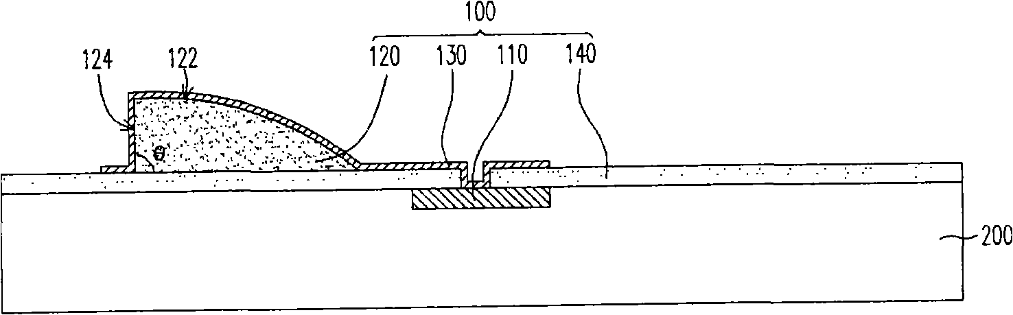
[0082] figure 1 It is a sectional view of the contact and the structure of the embodiment of the present invention. Please refer to figure 1 , the contact structure 100 of this embodiment is disposed on the substrate 200 . The contact structure 100 includes a pad 110 , a polymer bump 120 and a conductive layer 130 . The pads 110 are located on the substrate 200 . The polymer bump 120 is disposed on the substrate 200 , and the polymer bump 120 has an arc-shaped surface 122 and a steep surface 124 connected to the arc-shaped surface 122 . The included angle θ between the steep surface 124 and the substrate 200 is 30° to 150°. The conductive layer 130 covers the polymer bump 120 and is electrically connected to the pad 110 .
[0083] Based on the above, the polymer bump 120 of this embodiment has an arc-shaped surface 122 and a steep surface 124 connected to the arc-shaped surface 122 . Here, the steep surface 124 of the polymer bump 120 and the surface of the substrate 200 ...
no. 2 example
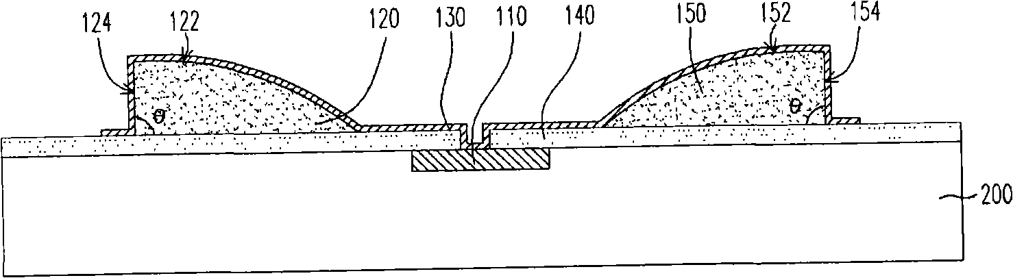
[0093] Figure 13 to Figure 24 It is a cross-sectional view of the contact structure of the second embodiment of the present invention. Figure 13 to Figure 24 The second embodiment shown is the same as Figure 1 to Figure 12 The illustrated embodiment is similar except that Figure 13 to Figure 24 In the embodiment, the arc-shaped surface 122 of the polymer bump 120 of the contact structure 300 further has a plurality of concave-convex structures 122a, or, in addition to the arc-shaped surface 122 of the polymer bump 120 of the contact structure 300, there are more plurality of concave-convex structures In addition to the structure 122a, the arc-shaped surface 152 of the polymer bump 150 of the contact structure 300 also has a plurality of concave-convex structures 152a.
[0094] Therefore, when a bonding material is disposed between the substrate 200 and another substrate and the polymer bump 120 is intended to be in contact with another substrate, the concave-convex struc...
no. 3 example
[0096] Figure 25 to Figure 36 It is a cross-sectional view of the contact structure of the third embodiment of the present invention. Figure 25 to Figure 36 The third embodiment shown is the same as Figure 1 to Figure 12 The illustrated embodiment is similar except that Figure 25 to Figure 36 In the embodiment, the arc-shaped surface 122 of the polymer bump 120 of the contact structure 400 is concave toward the direction of the substrate 200, or, except that the arc-shaped surface 122 of the polymer bump 120 of the contact structure 400 is concave toward the substrate 200 In addition to the concave direction, the arc-shaped surface 152 of the polymer bump 150 of the contact structure 400 is also concave toward the direction of the substrate 200 . Thus, in Figure 25 to Figure 36 In the illustrated embodiment, the junction of the arc-shaped surface 122 and the vertical surface 124 of the polymer bump 120 is a sharp structure. The junction of the arc-shaped surface 152 a...
PUM
 Abstract
Description
Claims
Application Information
 - R&D Engineer
- R&D Manager
- IP Professional
- Industry Leading Data Capabilities
- Powerful AI technology
- Patent DNA Extraction
Browse by: Latest US Patents, China's latest patents, Technical Efficacy Thesaurus, Application Domain, Technology Topic.
© 2024 PatSnap. All rights reserved.Legal|Privacy policy|Modern Slavery Act Transparency Statement|Sitemap