Supercharge Your Innovation With Domain-Expert AI Agents!

Domain structure of frequency synthesizer chip

A technology of frequency synthesizer and layout structure, applied in instruments, semiconductor devices, electric solid-state devices, etc., can solve the problems of frequency synthesizer chip design failure, unreasonable layout design, etc., to achieve optimized design, reasonable location layout, and reduced size the effect of interference

Inactive Publication Date: 2009-11-25
INST OF MICROELECTRONICS CHINESE ACAD OF SCI
View PDF0 Cites 0 Cited by
  • Summary
  • Abstract
  • Description
  • Claims
  • Application Information

AI Technical Summary

Problems solved by technology

[0003] In order to solve the problem of frequency synthesizer chip design failure due to unreasonable layout design, the present invention provides a frequency synthesizer chip layout structure, the frequency synthesizer chip layout consists of a first layout area, a second layout area, a second layout area The third layout area, the fourth layout area, the fifth layout area and the sixth layout area; the first layout area, the second layout area, the third layout area, the fourth layout area and the fifth layout area are located at the frequency The center of the synthesizer chip layout; the first layout area is connected to the second layout area, the second layout area is connected to the fifth layout area, the second layout area is connected to the fourth layout area, and the fourth layout area is connected to the fifth layout area. The layout area is connected to the third layout area, and the fourth layout area is connected to the fifth layout area; the sixth layout area is evenly distributed on the periphery and four corners of the frequency synthesizer chip layout

Method used


Image

  • Domain structure of frequency synthesizer chip

Examples


Embodiment Construction

[0012] In order to make the object, technical solution and advantages of the present invention clearer, the implementation manner of the present invention will be further described in detail below in conjunction with the accompanying drawings.

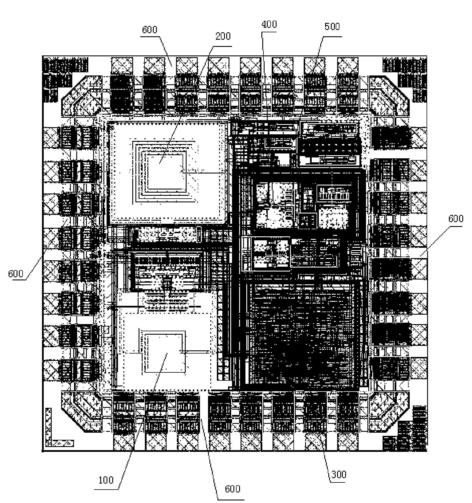
[0013] see figure 1 , this embodiment takes the S-band Fractional-N frequency synthesizer as an example to illustrate the frequency synthesizer chip layout structure provided by the embodiment of the present invention. The frequency synthesizer chip layout consists of a first layout area 100, a second layout area 200, The third layout area 300, the fourth layout area 400, the fifth layout area 500 and the sixth layout area 600; the first layout area 100, the second layout area 200, the third layout area 300, the fourth layout area 400 and the sixth layout area The fifth layout area 500 is located in the center of the frequency synthesizer chip layout; the first layout area 100 is connected to the second layout area 200, the second layo...


PUM


Abstract

This invention discloses a domain structure of frequency synthesizer chip, belonging to the technical field of the integrated circuit design. The domain of frequency synthesizer chip is composed of a first domain area, a second domain area, a third domain area, a fourth domain area, a fifth domain area and a sixth domain area. The first domain area, the second domain area, the third domain area, the fourth domain area and the fifth domain area are located at the centre of the domain of frequency synthesizer chip. The first domain area is connected with the second domain area. The second domain area is connected with the fifth domain area. The second domain area is connected with the fourth domain area. The fourth domain area is connected with the third domain area. The fourth domain area is connected with the fifth domain area. The sixth domain area is uniformed distributed at four sides and four angles of the domain of frequency synthesizer chip. Each domain area distribution of the domain of frequency synthesizer chip of this invention is fixed; the position distribution is reasonable; the design of the frequency synthesizer chip is optimized. Therefore, the interference of the digital noise to the analogy / radiation circuit is reduced so as to make the digital analogy signals not mutually interfere.

Description

technical field [0001] The invention relates to the technical field of integrated circuit design, in particular to a frequency synthesizer chip layout structure. Background technique [0002] With the development of wireless communication technology, frequency synthesizers are used more and more widely as local oscillators. The disadvantage of the traditional integer-N frequency synthesizer is that the frequency resolution is equal to the reference frequency. However, in many application systems, the frequency resolution of the frequency synthesizer is required to be relatively high. The Fractional-N frequency synthesizer achieves a smaller step than any single-ring integer frequency synthesizer under the condition that the reference frequency remains unchanged, thus solving the limitation of low frequency resolution of the traditional integer frequency synthesizer. However, due to the existence of a large number of digital units, analog units and radio frequency units in t...

Claims


Application Information

Patent Timeline
Patent Type & Authority Applications(China)
IPC IPC(8): G06F17/50H01L27/02H03L7/18
Inventor 郭桂良阎跃鹏杜占坤
Owner INST OF MICROELECTRONICS CHINESE ACAD OF SCI
Features
  • R&D
  • Intellectual Property
  • Life Sciences
  • Materials
  • Tech Scout
  • Unparalleled Data Quality
  • Higher Quality Content
  • 60% Fewer Hallucinations
Learn More