MOS transistor noise model formation method, device and circuit simulation method

A MOS transistor and noise model technology, applied in electrical digital data processing, special data processing applications, instruments, etc., can solve the problems that affect the accuracy of circuit design, do not consider the effect of temperature change of MOS transistors, and affect circuit performance.

Inactive Publication Date: 2009-12-02
SEMICONDUCTOR MANUFACTURING INTERNATIONAL (BEIJING) CORP
View PDF0 Cites 12 Cited by
  • Summary
  • Abstract
  • Description
  • Claims
  • Application Information

AI Technical Summary

Problems solved by technology

[0010] Therefore, the noise model of the MOS transistor model of the BSIM of the prior art only describes the noise characteristics of the MOS transistor at room temperature, without considering the influence of the temperature change effect of the MOS transistor, which is different from the fact that the channel conductivity type is n-type The current noise density of MOS transistors at different temperatures behaves differently and inconsistently
At the same time, because the noise model of the MOS transistor in the prior art does not consider the relationship between temperature and noise, the accuracy of the circuit design will be affected during the circuit design and simulation process, thereby affecting the performance of the entire circuit

Method used


Image

  • MOS transistor noise model formation method, device and circuit simulation method
  • MOS transistor noise model formation method, device and circuit simulation method
  • MOS transistor noise model formation method, device and circuit simulation method

Examples


Embodiment Construction

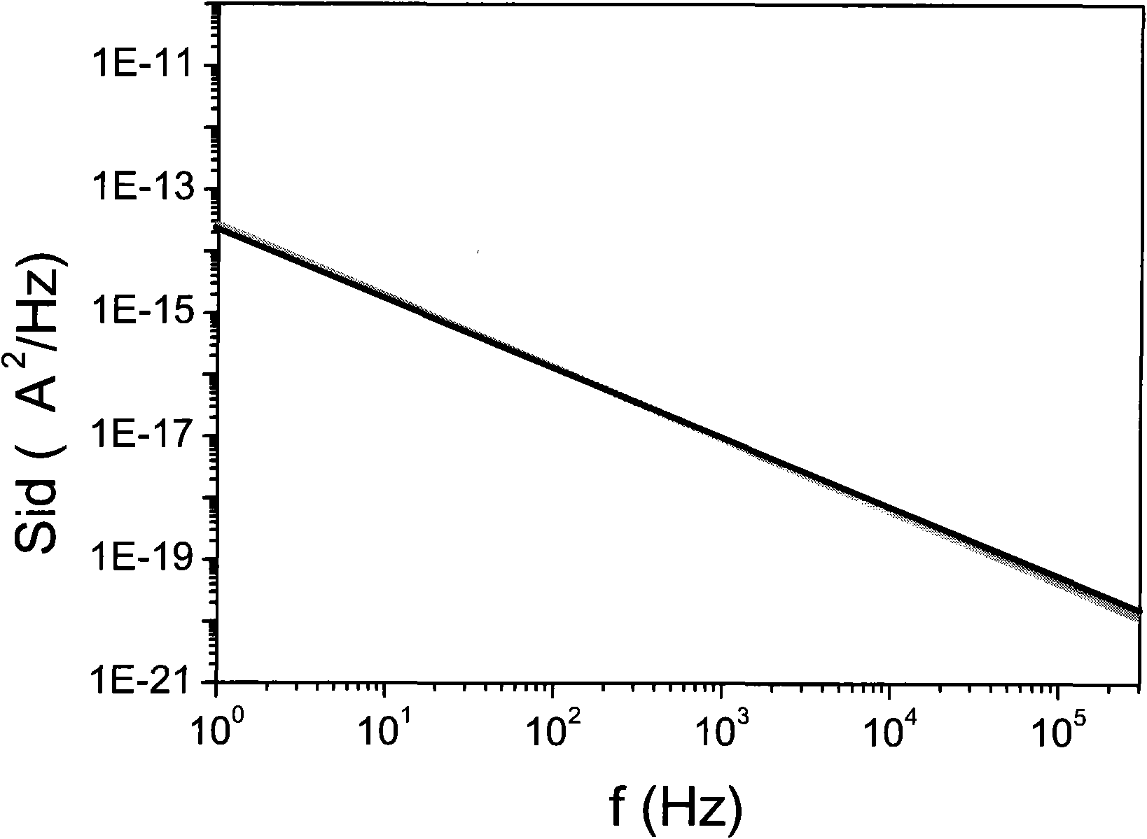
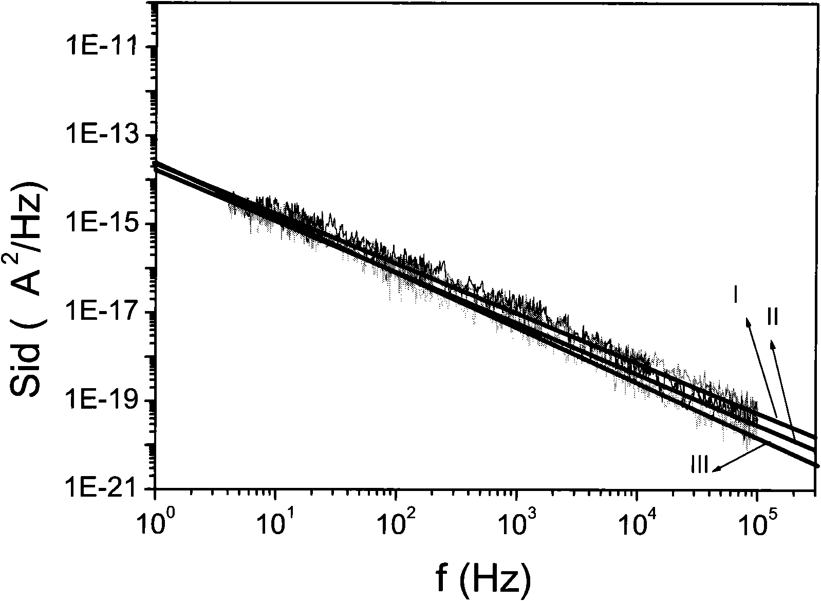
[0033] The present invention obtains normal temperature coefficient K by obtaining f0 and A f0 and the values ​​of parameters A and B, adding the influence of temperature to the noise model of the MOS transistor makes the noise model of the MOS transistor more accurate. The relationship between current noise figure (Sid) and frequency (f) in operation is more consistent.

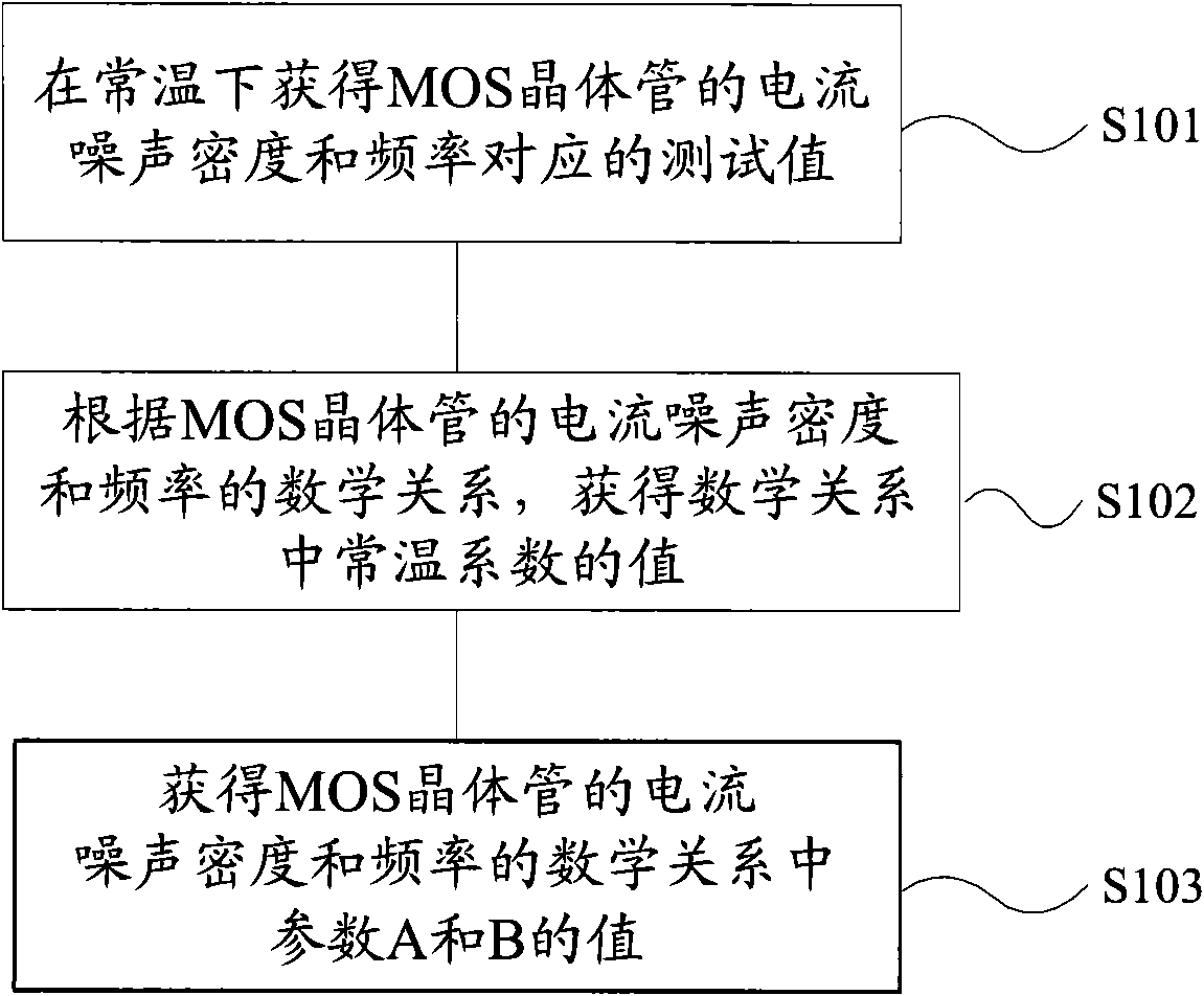
[0034] First, the present invention provides a schematic flow chart of a specific embodiment of a method for forming a noise model of a MOS transistor, referring to image 3 , including the following steps:

[0035] Step S101 is executed to obtain test values ​​corresponding to the current noise density Sid and the frequency f of the MOS transistor at room temperature.

[0036] Execute step S102, according to the mathematical relationship between the current noise density Sid of the MOS transistor and the frequency f Sid = { ...


PUM


Abstract

An MOS transistor noise model formation method comprises: obtaining current noise density Sid of the MOS transistor and test value corresponding to frequency f at normal temperature; obtaining values of normal temperature coefficient Kf0 and Af0 according to the mathematical relation of the current noise density Sid of the MOS transistor and testing value corresponding to frequency f as shown in the graph; changing the test temperature to obtain the current noise density Sid of the MOS transistor and testing value corresponding to frequency f at different temperatures; obtaining Kf0.[1+B.(T / Tn-1)] and Af0.[1+A.(T / Tn-1)] values corresponding to different test temperatures according to the mathematical relation of the current noise density Sid and testing value corresponding to frequency f; and fitting temperature T and Kf0.[1+B.(T / Tn-1)] and Af0.[1+A.(T / Tn-1)] values to obtain values of parameter A and parameter B. The invention also provides an MOS transistor noise model formation device and a circuit simulation method, which cause the simulation result in the circuit design to be more reliable by adding temperature influence in the noise model of the MOS transistor.

Description

technical field [0001] The invention relates to the technical field of semiconductors, in particular to a method for forming a MOS transistor noise model, a device and a circuit simulation method. Background technique [0002] With the continuous shrinking of the device size in CMOS technology, for analog circuits, the 1 / f noise parameter of the drain current at the gate voltage becomes more and more important. The greater the 1 / f noise of the drain current, the amplifier, digital The smaller the signal-to-noise ratio (SNR) in an analog-to-analog converter or an analog-to-digital converter. Therefore, in circuit design, it is necessary to accurately control the 1 / f noise parameter of the drain current, and the key to controlling the 1 / f noise parameter lies in the accuracy of the model used. [0003] At present, the popular MOS transistor model is mainly the BSIM (Berkeley Short-channelIGFET Model) model, and the SPICE (Simulation Program with Integrated Circuit Emphasis) m...

Claims


Application Information

Patent Timeline
IPC IPC(8): G06F17/50
Inventor 赵芳芳
Owner SEMICONDUCTOR MANUFACTURING INTERNATIONAL (BEIJING) CORP
Why Eureka
Try Eureka