Frequency dithering circuit and frequency dithering method as well as application thereof in switch power supply

A technology of frequency jitter and circuit, applied in the direction of electric pulse generator circuit, pulse frequency/rate modulation, output power conversion device, etc., can solve the problems of increasing PCB board volume and cost, and achieve EMI average noise reduction and cost reduction Effect

Inactive Publication Date: 2010-01-27
HANGZHOU SILAN MICROELECTRONICS
View PDF1 Cites 17 Cited by
  • Summary
  • Abstract
  • Description
  • Claims
  • Application Information

AI Technical Summary

Problems solved by technology

In practice, filtering is often used to reduce electromagnetic interference, but this method requ

Method used


Image

  • Frequency dithering circuit and frequency dithering method as well as application thereof in switch power supply
  • Frequency dithering circuit and frequency dithering method as well as application thereof in switch power supply
  • Frequency dithering circuit and frequency dithering method as well as application thereof in switch power supply

Examples


Embodiment Construction

[0056] The content of the present invention will be further described below in conjunction with the accompanying drawings.

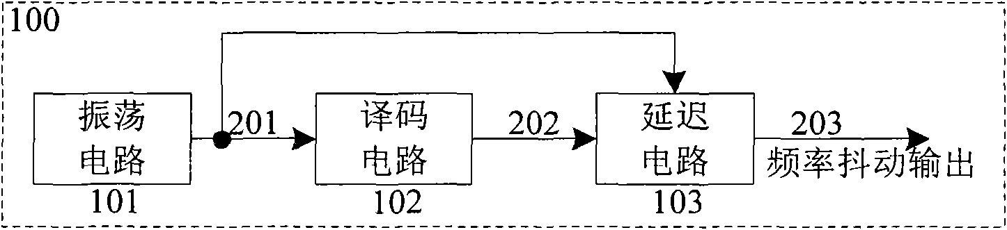
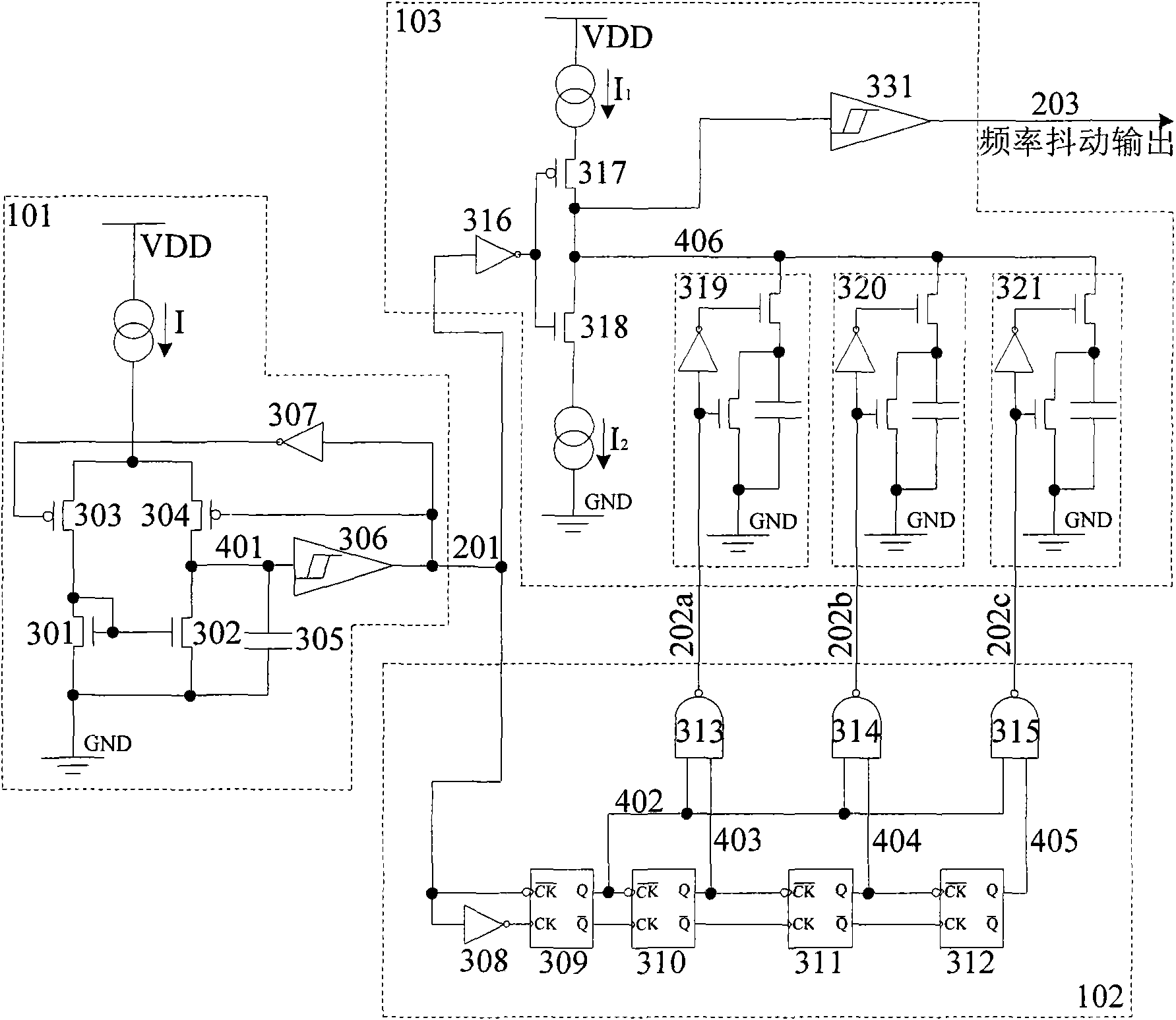
[0057] Such as figure 1 Shown is the frequency dithering circuit 100 of the present invention, comprising:

[0058] An oscillation circuit 101 that generates an oscillation frequency output signal 201;

[0059] Decoding circuit 102, the oscillating frequency output signal 201 controls the decoding circuit 102 to generate a number of pulse output signals 202, and in this embodiment, three pulse output signals are generated as an example for illustration;

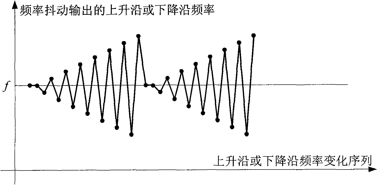
[0060] Delay circuit 103, the oscillating frequency output signal 201 passes through the delay circuit 103 to generate a frequency jitter output signal 203, the frequency jitter output signal 203 is delayed for a period of time compared with the oscillating frequency output signal 201, and the pulse output signal 202 controls the frequency The delay time for dithering the output signal.

[0061] im...


PUM


Abstract

The invention provides a frequency dithering circuit and a frequency dithering method. The frequency dithering circuit comprises an oscillatory circuit, a decoding circuit and a delay circuit, wherein the oscillatory circuit generates an oscillatory frequency output signal; the oscillatory frequency output signal controls the decoding circuit to generate a plurality of pulse output signals; and the delay circuit generates a frequency dithering output signal when the oscillatory frequency output signal passes by the delay circuit; the frequency dithering output signal delays for a period of time compared with the oscillatory frequency output signal; and the pulse output signals control the delay time of the oscillatory frequency output signal. The invention applied in a switch power supply can reduce the EMI average noise of the switch power supply and has energy spectrum density planarization.

Description

technical field [0001] The invention relates to the field of switching power supplies, in particular to frequency jitter technology in integrated circuits. Background technique [0002] Due to the high-frequency switching of the switching power supply voltage regulator circuit, the circuit generates electromagnetic interference (EMI). EMI noise can be transmitted through the input AC power line, and can also be transmitted through radiation, which will affect other electronic instruments, such as communication tools, The normal work of household appliances, automatic control equipment, etc. [0003] In order to control electromagnetic interference (EMI), control standards for radiated energy are stipulated to ensure that various instruments will not affect normal work due to mutual interference. In practice, filtering is often used to reduce electromagnetic interference, but this method requires external capacitors and inductors on the chip, which increases the size and cos...

Claims


Application Information

Patent Timeline
IPC IPC(8): H02M1/44H02M3/335H03K3/023
CPCH03K7/06H02M1/44H04B2215/067H04B15/04H03K3/84G06F1/10
Inventor 周伟江姚云龙
Owner HANGZHOU SILAN MICROELECTRONICS
Why Eureka
Try Eureka