Method for manufacturing printed circuit board edge connector

A manufacturing method and gold finger technology, which is applied in the directions of printed circuit, printed circuit manufacturing, and electrical connection formation of printed components, etc., can solve problems such as electroplating lead residues, and achieve the effect of solving electroplating lead residues

Active Publication Date: 2010-02-10
NEW FOUNDER HLDG DEV LLC +2
View PDF0 Cites 70 Cited by
  • Summary
  • Abstract
  • Description
  • Claims
  • Application Information

AI Technical Summary

Problems solved by technology

[0007] The invention provides a method for manufacturing gold fingers of printed circuit boards, which can solve the problem of residual electroplating leads of gold fingers of printed circuit boards

Method used


Image

  • Method for manufacturing printed circuit board edge connector
  • Method for manufacturing printed circuit board edge connector
  • Method for manufacturing printed circuit board edge connector

Examples


Embodiment 1

[0028] Such as Figure 4 As shown, the manufacturing method of printed circuit board golden finger of the present invention comprises steps:

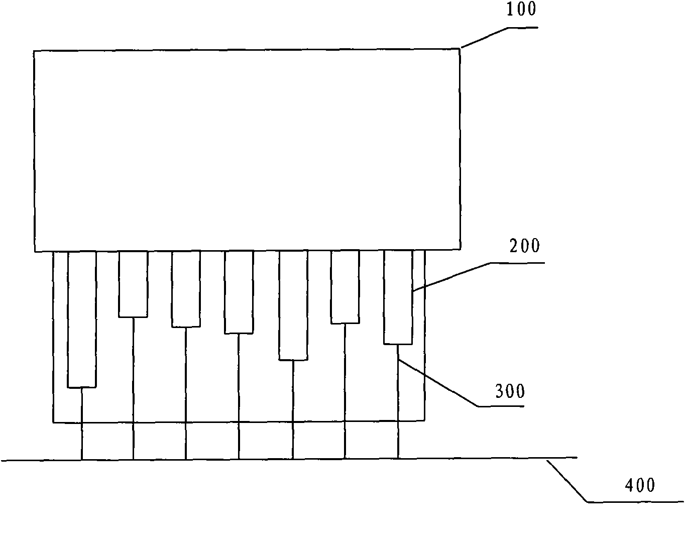
[0029] S 10. Form the gold finger electroplating lead and the gold finger area at one time on the printed circuit board, wherein the width of the adjacent part of the electroplating lead and the gold finger area is equal to the width of the gold finger area.

[0030] Such as Figure 5 As shown, when the printed wiring board 100 is transferred to the circuit pattern for the first time, the gold finger plating lead 300 and the gold finger area 600 on the printed wiring board 100 are formed once, and the electroplating lead 300 and the gold finger area The width of the adjacent portion 600 is equal to the width of the golden finger area 600 . In this embodiment, the gold finger electroplating lead 300 is preferably designed to be of equal width throughout, but the present invention is not limited thereto.

[0031] S20. Coating a coverin...

Embodiment 2

[0038] This embodiment provides a method for manufacturing a multi-stage graded leadless golden finger. The method for manufacturing the graded leadless gold finger in this embodiment will be described in detail below in conjunction with the accompanying drawings.

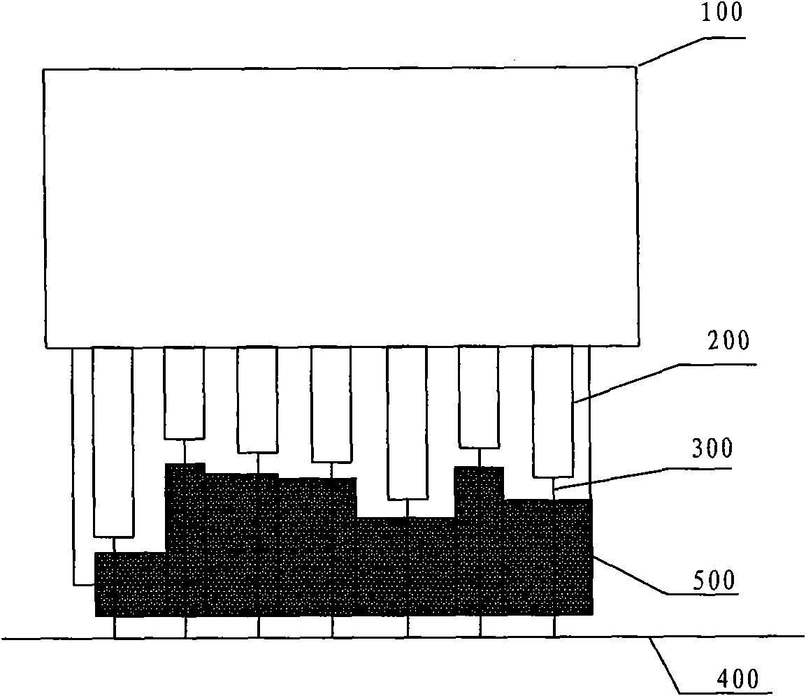
[0039] The manufacturing method of the graded leadless gold finger in this embodiment is basically the same as the manufacturing method of the printed circuit board leadless gold finger in the first embodiment above. The difference is that if Figure 9 As shown, when coating the cover, the electroplating lead 300 is coated with dry film or anti-plating ink 500; the gold finger area 600 is segmentally coated with anti-plating ink 500 to form a multi-stage graded gold finger electroplating reserved area 700 ; Cover the blue tape on the circuit pattern on the printed circuit board 100 except the gold finger area and the electroplated lead. When covering the anti-plating ink, it should also be noted that the length o...

Embodiment 3

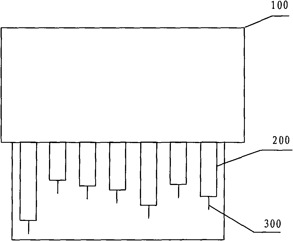
[0042] Such as Figure 11 As shown, in this embodiment, the connecting area between the gold finger plating lead 300 and the gold finger region 600 is made to have the same width, and the design of the connection area between the gold finger plating lead 300 and the main lead 400 can be smaller than the width of the gold finger region 600 ; By covering the electroplating ink 500 to the gold finger electroplating lead wire 300, a reserved area for gold finger electroplating is formed; before gold plating, other circuit pattern parts (except the gold finger and wire area) on the printed circuit board are covered with dry film or paste Protect it with blue tape, and then electroplate nickel and gold. After the electroplating is completed, remove the blue tape of the anti-plating ink and graphic part; and cover other circuit graphic parts (except gold finger wires) on the printed circuit board. The dry film is specially etched for gold finger wires, and the production of leadless ...


PUM


Abstract

The invention discloses a method for manufacturing a printed circuit board edge connector, relates to the field of manufacturing process for a printed circuit board, and can solve the residue problemsof an edge connector plating lead of the printed circuit board. The method for manufacturing the printed circuit board edge connector comprises the following steps: forming the edge connector platinglead and an edge connector area on the printed circuit board once, wherein the width of adjacent parts of the edge connector plating lead and the edge connector area is equal to the width of the edgeconnector area; coating a covering substance to form an edge connector plating reserved area, and plating the edge connector plating reserved area to form the edge connector; and removing the covering substance, and etching the edge connector to obtain the edge connector without the plating lead. The method is suitable for manufacturing the edge connector without the lead for the printed circuitboard.

Description

technical field [0001] The invention relates to the field of manufacturing technology of a printed circuit board (PCB), in particular to a method for manufacturing a golden finger of a printed circuit board. Background technique [0002] Gold finger (edge ​​connector) is used for the connection between printed circuit boards, which can connect circuits and transmit signals. On the printed circuit board near the edge of the board, many rectangular metal contacts are arranged in rows, and the metal contacts are formed by electroplating a layer of nickel gold on the copper pad. These metal contacts are part of the printed circuit board wiring. Because of their nickel-gold-plated surface and their shape resembling fingers, they are called gold fingers. The nickel gold on the surface of the gold finger can improve the insertion resistance, conductivity and oxidation resistance of this part. When using, just insert the golden finger position on the printed circuit board into the...

Claims


Application Information

Patent Timeline
Patent Type & Authority Applications(China)
IPC IPC(8): C25D5/02H05K3/18H05K3/40H01R12/16
Inventor 朱兴华
Owner NEW FOUNDER HLDG DEV LLC
Why Eureka
Try Eureka