Method for manufacturing circuit board layer-adding structure

一种增层结构、制造方法的技术,应用在微电子领域,能够解决精细线路成本高等问题,达到降低材料成本、降低基板成本、提高化学活性的效果

Active Publication Date: 2014-01-01
NAT CENT FOR ADVANCED PACKAGING CO LTD
View PDF6 Cites 33 Cited by
  • Summary
  • Abstract
  • Description
  • Claims
  • Application Information

AI Technical Summary

Problems solved by technology

[0043] It can be seen that the SAP process is very expensive for making fine lines with a line width less than 50 microns.

Method used


Image

  • Method for manufacturing circuit board layer-adding structure
  • Method for manufacturing circuit board layer-adding structure
  • Method for manufacturing circuit board layer-adding structure

Examples


Embodiment Construction

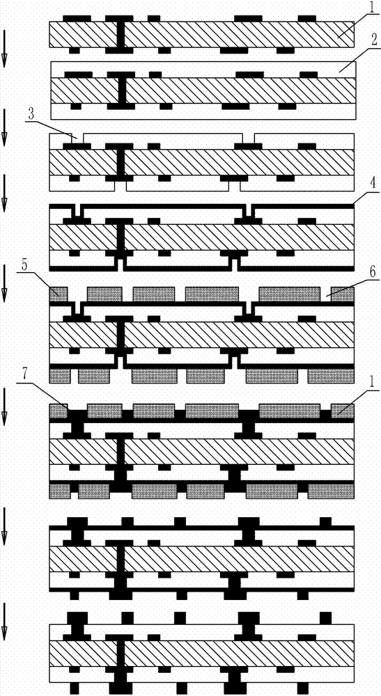
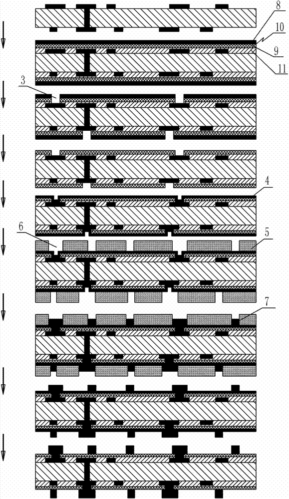
[0094] The present invention will be further described in conjunction with accompanying drawing:

[0095] Figure 6 It is the semi-addition process flow of the present invention;

[0096] A method for manufacturing a circuit board build-up structure, comprising the following steps:

[0097] (1), see Figure 7 , production of inner layer circuit: make inner layer circuit 1, make metallized via hole 3 on the core board 2, make copper circuit 4 on both sides of the core board 2, the inner layer circuit of the package carrier board is wider, usually use the subtractive method to Finish;

[0098] (2), see Figure 8 , press the copper foil 4 and the prepreg 5 on both sides of the inner circuit 1 and solidify: press the copper foil 5 and the prepreg 6 on both sides of the inner circuit 1, and transfer the low-roughness structure on the surface of the copper foil 5 to the prepreg 6 ;

[0099] (3), see Figure 9 , Copper reduction: Thin the copper foil 5 to a thickness of 3um. ...


PUM


Abstract

The invention provides a method for manufacturing a circuit board layer-adding structure. Manufacture of a fine circuit with the width smaller than 50 micrometers is achieved, use of insulation materials with high cost is avoided, so that the process cost of a substrate is reduced, and therefore cost of the substrate is reduced. The method comprises the following steps that (1) an inner-layer circuit is manufactured; (2) copper foil and prepreg are pressed and solidified; (3) laser drilling is conducted; (4) smear removal is conducted; (5) surface copper is removed; (6) plasma activating treatment is conducted on the surface of a circuit board; (7) electroless copper plating is conducted; (8) photoetching is conducted; (9) electroplating is conducted; (10) membrane stripping is conducted; (11) flash etching is conduced. According to the method, generally-used medium material PP is adopted; through the improvement of the SAP technical method, the chemical activity of the surface of the PP is improved, electroless copper plating is directly conducted on the surface of the PP, the binding force of an electroless copper plating layer is improved, so that the SAP machining requirements of the fine circuit are satisfied, and meanwhile the technical cost of the substrate is reduced to a great extent.

Description

technical field [0001] The invention relates to a method for manufacturing or processing a semiconductor or solid device in the technical field of microelectronics, in particular to a method for manufacturing a circuit board build-up structure. Background technique [0002] With the development of large-scale integrated circuits, the lines are getting thinner and thinner. 22nm technology has entered mass production, and the thinning of lines has brought unprecedented challenges to equipment and processes. In order to improve the chip density and signal processing capability per unit area, 3D packaging came into being. People put forward the concept of three-dimensional packaging, which involves three-dimensional integrated packaging of chips, and stacking chips to form three-dimensional packaging to improve the density per unit area. Packing density. [0003] The development of three-dimensional high-density packaging has higher and higher requirements for organic substrate...

Claims


Application Information

Patent Timeline
Patent Type & Authority Applications(China)
IPC IPC(8): H05K3/46
CPCH05K3/4644H05K3/0035H05K3/0055H05K3/108H05K2203/0353H05K2203/143Y10T29/49167
Inventor 于中尧孙瑜崔志勇方志丹石桂涵刘文龙
Owner NAT CENT FOR ADVANCED PACKAGING CO LTD
Why Eureka
Try Eureka