Ultra-multi-layer ultra-deep-cavity LTCC substrate manufacturing technology
A manufacturing process, ultra-multi-layer technology, applied in multi-layer circuit manufacturing, printed circuit manufacturing, circuit lamination, etc.
- Summary
- Abstract
- Description
- Claims
- Application Information
AI Technical Summary
Problems solved by technology
Method used
Image
Examples
Embodiment Construction
[0052] The present invention will be further described below in conjunction with the accompanying drawings. The following examples are only used to illustrate the technical solution of the present invention more clearly, but not to limit the protection scope of the present invention.
[0053] 1. Technical solution
[0054] The concise technical scheme of the patent application for the present invention is:
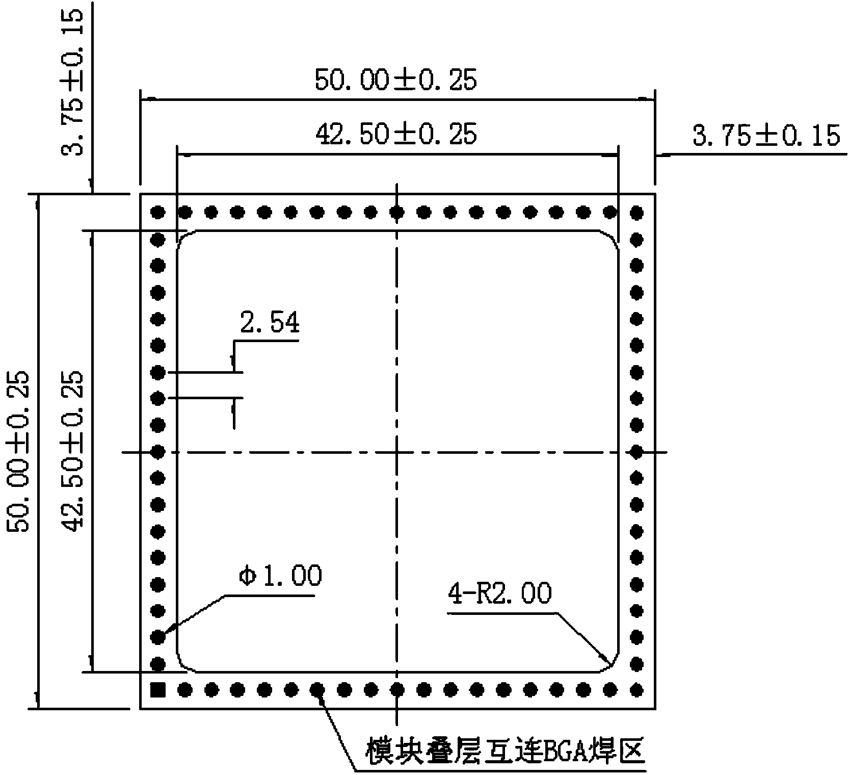
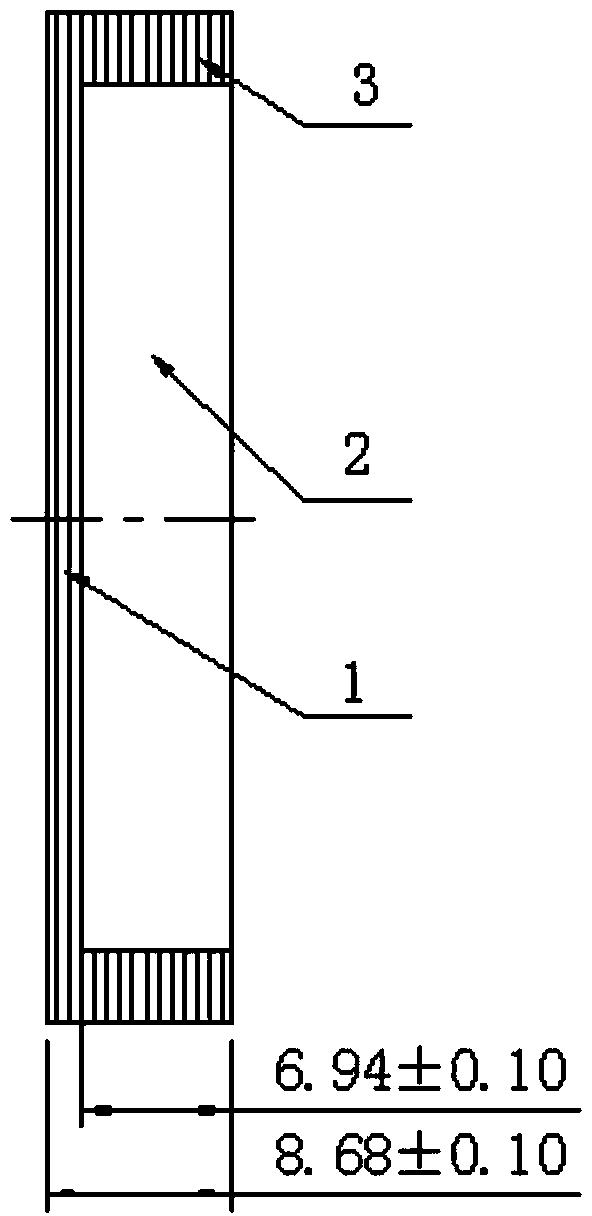
[0055] 1) LTCC substrate with cavity ( Figure 1a , Figure 1b , unit substrate) a total of 90 layers of raw porcelain, of which the bottom plate 1 is 18 layers, and the cavity 2 is 72 layers. The size is 42.50mm (length) × 42.50mm (width) × 6.94mm (depth); the upper and lower limit deviation of the length and width of the substrate and cavity is 0.25mm, the upper and lower limit deviation of the substrate thickness and cavity depth is 0.10mm, and the cavity The upper and lower limit deviation of side wall 3 wall thickness is 0.15mm;
[0056] 2) DuPont 951PT type LTCC ...
PUM
 Abstract
Description
Claims
Application Information


