

Semiconductor device, its manufacturing method and optical pickup module
A manufacturing method, semiconductor technology, applied in the direction of semiconductor devices, semiconductor/solid-state device components, radiation control devices, etc.
- Summary
- Abstract
- Description
- Claims
- Application Information
AI Technical Summary
Problems solved by technology
Method used
Image

Examples
no. 1 approach
[0067] -Semiconductor device-
[0068] The semiconductor device according to the first embodiment is a photodetector using an integrated light receiving element as a semiconductor element. It should be mentioned that light-receiving elements such as photodiodes, phototransistors, and photosensitive integrated circuits (ICs) can be used as semiconductor elements, and light-emitting elements such as LEDs (semiconductor light-emitting diodes) and semiconductor laser elements can also be used as semiconductor elements.
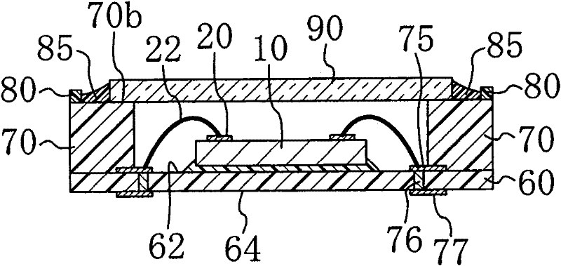
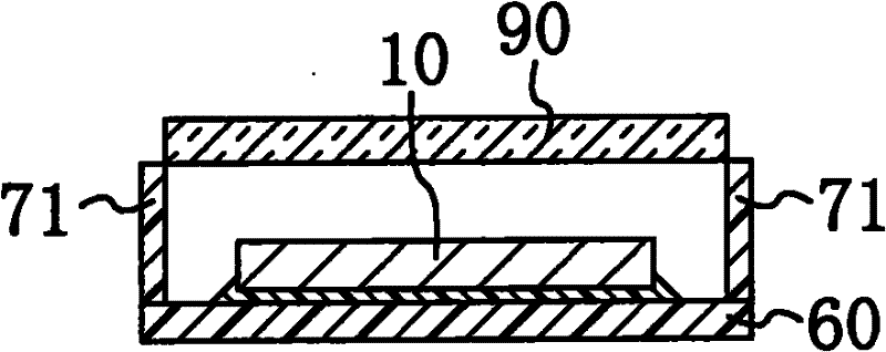
[0069] As shown in FIG. 1 , in a semiconductor device 1 of this embodiment, a semiconductor element 10 is housed in a groove of a package 50 having a U-shaped cross section and covered by a transparent flat cover 90 . Fig. 2 (a) to Fig. 2 (d) also show the semiconductor device 1 in this embodiment, but for the convenience of explanation, what Fig. 2 (a) shows is the situation after removing the cover body 90, the cover body 90 Not shown in this Fig. 2(a).
[007...
no. 2 approach
[0097] The semiconductor device according to the second embodiment differs from the semiconductor device 1 according to the first embodiment only in that the dam 80 is removed from the semiconductor device according to the second embodiment, and is the same in other respects. Therefore, only the differences from the first embodiment will be described below.
[0098] FIG. 7 is a cross-sectional view showing the manufacturing process of the semiconductor device 2 according to this embodiment. Figure 7(a) to Figure 7(e) The manufacturing steps shown are the same as the manufacturing steps of the semiconductor device 1 according to the first embodiment shown in FIG. 3 . In this embodiment, the dams 80, 80, . At this time, the dams 80, 80, . . . are made of a material that the adhesive 85 will not stick to.
[0099]Therefore, as shown in FIG. 6 , the semiconductor device 2 in this embodiment uses a package 50 , a semiconductor element 10 , and a lid 90 as in the first embodiment...
no. 3 approach
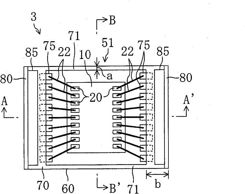
[0102] The semiconductor device according to the third embodiment is configured by adding the second protrusion to the semiconductor device 1 according to the first embodiment. Other points are the same as those of the first embodiment. Therefore, only the differences from the first embodiment will be described below.
[0103] As shown in FIGS. 8 and 9 , in the semiconductor device 3 in this embodiment, first protrusions 70 , 70 and second protrusions 71 , 71 are provided. In the semiconductor device 1 according to the first embodiment, the side surfaces of the semiconductor device 1 which are open to the outside are closed by the second protrusions 71 , 71 , and the semiconductor element 10 is in a sealed state. The direction in which the second protrusions 71 , 71 extend is perpendicular to the direction in which the first protrusions 70 , 70 extend. It should be mentioned that, for the convenience of explanation, FIG. 9( a ) shows the state where the cover body 90 is remo...
PUM
| Property | Measurement | Unit |
|---|---|---|
| wavelength | aaaaa | aaaaa |
| wavelength | aaaaa | aaaaa |
Abstract
Description
Claims
Application Information