Structure and method for packaging organic electroluminescence component
An electroluminescent device, packaging structure technology, applied in the direction of electric solid devices, electrical components, semiconductor devices, etc., can solve the problem of desorption and release of water vapor and oxygen, penetration of device sealing materials, and internal materials of devices containing water vapor and oxygen and other problems to achieve the effect of reducing adsorption and dissolution, improving performance and life, and reducing outgassing
- Summary
- Abstract
- Description
- Claims
- Application Information
AI Technical Summary
Problems solved by technology
Method used
Image
Examples
Embodiment 1
[0066] Example 1 Vacuum-encapsulated organic electroluminescent device with glass substrate and cover plate
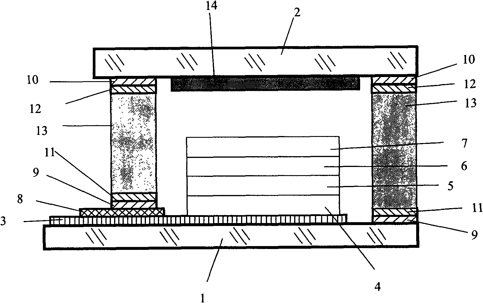
[0067] The packaging structure of this device is as figure 2 shown.
[0068] Manufacturing process of glass substrate 1:
[0069] Step 1, plating an ITO thin film electrode layer 3 on the upper surface of the substrate glass 1, the plating method is DC magnetron sputtering or radio frequency magnetron sputtering.
[0070] In step 2, an insulating film 8 is plated on the surface of the ITO thin film electrode layer 3 corresponding to the sealing position to cover the surface of the ITO thin film electrode layer 3 at the sealing position. The coating method is one of vacuum evaporation coating, electron beam evaporation coating and reactive sputtering coating. The film thickness of the insulating layer is 50-200nm.
[0071] Step 3, at the position to be sealed at the frame of the glass substrate 1, on the surface of the glass part including the part with the insulat...
Embodiment 2
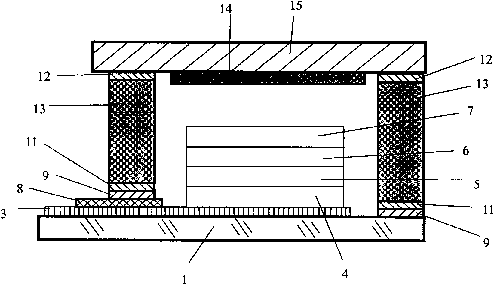
[0087] Example 2 A vacuum-encapsulated organic electroluminescence device in which the substrate is glass and the cover plate is metal
[0088] Manufacturing process of glass substrate 1:
[0089] Same as 1 embodiment 1 process.
[0090] The manufacturing process of the metal cover plate 15:
[0091] Step 1: At the sealing position of the metal cover plate 15, the transition layer thin films 11 and 12 are plated by methods such as DC magnetron sputtering, ion plating and vacuum evaporation. The materials of the transition layer are metals such as Au, Ag, Pt and Cu. The thickness of the transition layer is 50-200nm.
[0092] Step 2: On the center of the inner surface of the metal cover plate 15 and on the metal surface in the vicinity, vacuum evaporation, electron beam evaporation and other methods are used to plate an evaporative getter layer.
[0093] Device sealing process:
[0094] Same as embodiment 1 process.
PUM
| Property | Measurement | Unit |
|---|---|---|
| thickness | aaaaa | aaaaa |
| thickness | aaaaa | aaaaa |
| melting point | aaaaa | aaaaa |
Abstract
Description
Claims
Application Information
 - R&D
- Intellectual Property
- Life Sciences
- Materials
- Tech Scout
- Unparalleled Data Quality
- Higher Quality Content
- 60% Fewer Hallucinations
Browse by: Latest US Patents, China's latest patents, Technical Efficacy Thesaurus, Application Domain, Technology Topic, Popular Technical Reports.
© 2025 PatSnap. All rights reserved.Legal|Privacy policy|Modern Slavery Act Transparency Statement|Sitemap|About US| Contact US: help@patsnap.com


