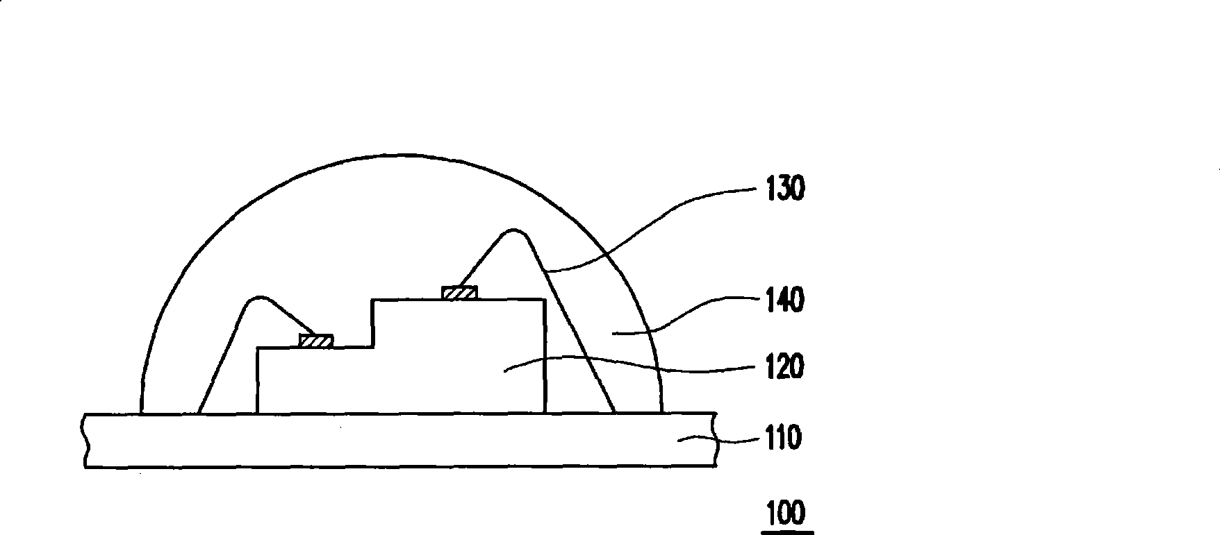
LED packager
A technology of light-emitting diodes and diodes, which is applied to electrical components, electric solid-state devices, circuits, etc., can solve problems such as light loss, and achieve the effect of improving luminous efficiency
- Summary
- Abstract
- Description
- Claims
- Application Information
AI Technical Summary
Problems solved by technology
Method used
Image

Examples
no. 1 example
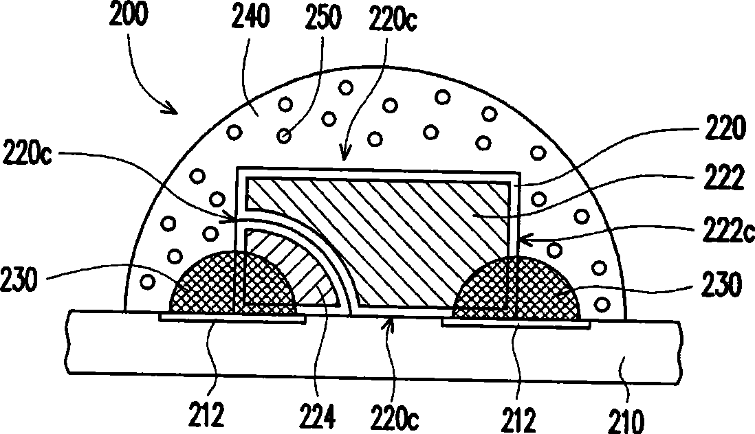
[0044] Figure 2A is a side view of the LED package according to the first embodiment of the present invention, and Figure 2B It is a three-dimensional schematic view of the LED package according to the first embodiment of the present invention. Please refer to Figure 2A and Figure 2B , the light emitting diode package 200 of this embodiment includes a carrier 210 , a light emitting diode chip 220 and a plurality of conductors 230 . The light emitting diode chip 220 has a front side 220a, a back side 220b and a plurality of sidewalls 220c connected between the front side 220a and the back side 220b, and one of the sidewalls 220c of the light emitting diode chip 220 faces the carrier 210 and is connected to the carrier 210 . In addition, the conductor 230 is electrically connected between the carrier 210 and the LED chip 220 .
[0045] In this embodiment, the carrier 210 can be a circuit board with a plurality of pads 212 , and the LED chip 220 is electrically connected...
no. 2 example
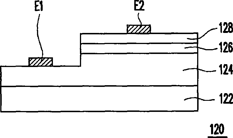
[0053] image 3 It is a side view of the LED package according to the second embodiment of the present invention. Please refer to image 3 The light emitting diode package 300 of this embodiment is similar to the light emitting diode package 200 of the first embodiment, but the main difference between the two lies in: the light emitting diode chip 320 and the light emitting diode chip 220 used in this embodiment. In detail, the LED chip 320 has a plurality of electrodes 322, 324, and these electrodes 322, 324 are distributed on the front side 320a and the back side 320b of the LED chip 320 respectively. In addition, the electrodes 322 and 324 are respectively electrically connected to the carrier 210 through the conductors 230 located on both sides of the LED chip 320 .
no. 3 example
[0055] Figure 4 It is a side view of the LED package according to the third embodiment of the present invention. Please refer to Figure 4 The light emitting diode package 400 of this embodiment is similar to the light emitting diode package 300 of the second embodiment, but the main difference between the two is that the number of light emitting diode chips 320 used in this embodiment is multiple ( Figure 4 are shown as 3). In detail, since the LED chips 320 are connected to the carrier 210 through the sidewalls 320c, the distance between the LED chips 320 (the distance from the center to the center of the two LED chips 320) can be effectively shortened, with good performance. light mixing efficiency. In other words, on the carrier 210 with the same area, this embodiment can accommodate a larger number of LED chips 320 to easily meet the requirement of high brightness output.
[0056] It is worth noting that in this embodiment, optical elements (such as light guide elem...
PUM
 Abstract
Description
Claims
Application Information
 - R&D
- Intellectual Property
- Life Sciences
- Materials
- Tech Scout
- Unparalleled Data Quality
- Higher Quality Content
- 60% Fewer Hallucinations
Browse by: Latest US Patents, China's latest patents, Technical Efficacy Thesaurus, Application Domain, Technology Topic, Popular Technical Reports.
© 2025 PatSnap. All rights reserved.Legal|Privacy policy|Modern Slavery Act Transparency Statement|Sitemap|About US| Contact US: help@patsnap.com