Method for performing gold backing on printed circuit board of Ku waveband microstrip type switch circuit

A technology for printed circuit boards and switch circuits, which is applied in the directions of printed circuit manufacturing, circuits, printed circuits, etc., can solve the problems of reduced isolation of switch circuits and complex electromagnetic fields, and achieves improved isolation, good repeatability, and avoidance of Effects of parasitic parameters

Active Publication Date: 2011-09-14
INST OF MICROELECTRONICS CHINESE ACAD OF SCI
View PDF0 Cites 0 Cited by
  • Summary
  • Abstract
  • Description
  • Claims
  • Application Information

AI Technical Summary

Problems solved by technology

Although the geometric structure of the microstrip line is not complicated, its electromagnetic field is quite complicated
Usually, the back of the printed circuit board is all backed with gold as the grounding base plate, but the microstrip line grounding base plate located on both sides of the circuit element will be connected together, which will cause the coupling effect of the microwave signal and reduce the isolation of the switching circuit.

Method used


Image

  • Method for performing gold backing on printed circuit board of Ku waveband microstrip type switch circuit
  • Method for performing gold backing on printed circuit board of Ku waveband microstrip type switch circuit
  • Method for performing gold backing on printed circuit board of Ku waveband microstrip type switch circuit

Examples


Embodiment Construction

[0028] In order to make the object, technical solution and advantages of the present invention clearer, the present invention will be described in further detail below in conjunction with specific embodiments and with reference to the accompanying drawings.

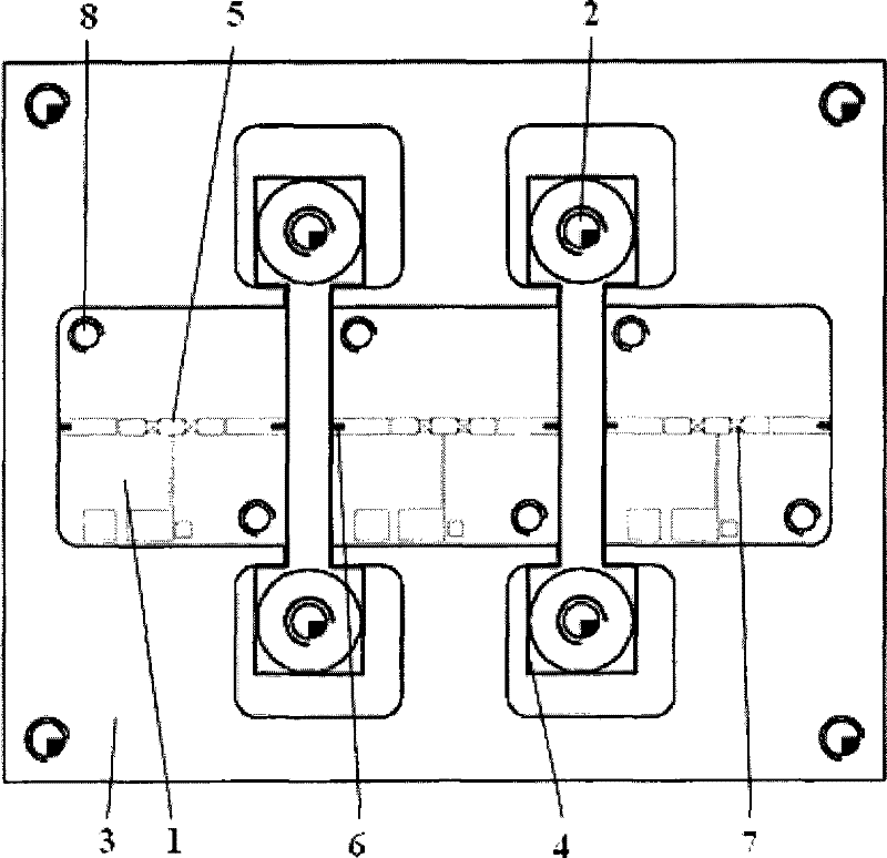
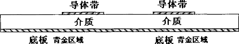
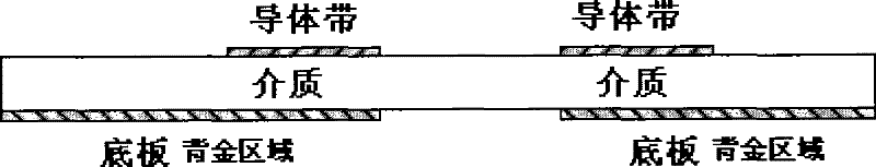
[0029] The method for carrying out back-gold on the printed circuit board of the Ku-band microstrip type switch circuit provided by the present invention is to selectively carry out back-gold on the microwave printed circuit board, and will be positioned between the microstrip lines on both sides of the circuit element. The grounded base plate, that is, the back gold part of the printed circuit board, is isolated to suppress the coupling effect of the microwave signal, thereby improving the isolation of the microwave switch circuit.

[0030] This method that the present invention provides to the printed circuit board of the Ku-band microstrip type switch circuit is carried out back gold method, when carrying out back-gold ...


PUM


Abstract

The invention discloses a method for performing gold backing on a printed circuit board of a Ku waveband microstrip type switch circuit, which selectively performs gold backing treatment on the printed circuit board in the process of performing the gold backing treatment on the printed circuit board in the Ku waveband microstrip type switch circuit so as to separate the part between the printed circuit board and the back face of a microstrip line grounded base plate, inhibit the coupling effect of microwave signals, avoid the introduction of more parasitic parameters in the circuit, and improve the isolation performance of the microstrip type switch circuit. The method effectively inhibits the coupling effect of the microwave signals, avoids the introduction of more parasitic parameters in the circuit, and finally improves the isolation performance of the microstrip type switch circuit. The method has the characteristics of simple manufacturing, good repeatability, low cost, wide application range and the like.

Description

technical field [0001] The invention relates to the technical field of design of a Ku-band microstrip switch circuit, in particular to a method for backing a printed circuit board of a Ku-band microstrip switch circuit. Background technique [0002] In radar transmitter systems, satellite communications and various communication and navigation electronic warfare systems, microwave switch circuits are widely used to realize the on, off or conversion of microwave signals. At present, when the microstrip switching circuit based on the PIN switching diode is applied in the microwave frequency band, there are some coupling effects caused by the microwave signal radiation due to the significant difference between the high-frequency microwave signal and the low-frequency AC or DC signal. As the frequency increases, this effect will have a greater impact on the circuit performance, resulting in a large gap between the theoretical design of the switching circuit and the actual debugg...

Claims


Application Information

Patent Timeline
Patent Type & Authority Patents(China)
IPC IPC(8): H01P1/10G06F17/50H05K3/00
Inventor 袁婷婷陈晓娟刘新宇陈中子陈高鹏阎跃鹏
Owner INST OF MICROELECTRONICS CHINESE ACAD OF SCI
Why Eureka
Try Eureka