Semiconductor structure and method of forming same

A semiconductor and barrier structure technology, applied in the field of semiconductor structures and their formation, can solve problems such as poor isolation performance of dielectric layers, and achieve the effects of improving isolation performance, improving interface state, and preventing separation

Active Publication Date: 2019-02-05
SEMICON MFG INT (SHANGHAI) CORP +1
View PDF4 Cites 0 Cited by
  • Summary
  • Abstract
  • Description
  • Claims
  • Application Information

AI Technical Summary

Problems solved by technology

[0004] However, when the barrier layer is formed, it is easy

Method used


Image

  • Semiconductor structure and method of forming same
  • Semiconductor structure and method of forming same
  • Semiconductor structure and method of forming same

Examples


Embodiment Construction

[0032] As mentioned in the background, semiconductor devices formed in the prior art have poor performance.

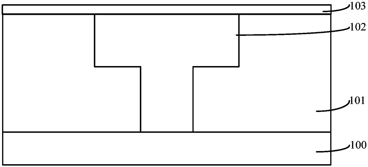
[0033] figure 1 is a schematic diagram of a semiconductor structure.

[0034] Please refer to figure 1 , providing a substrate 100, the substrate 100 has a dielectric layer 101, and the dielectric layer 101 has an opening (not shown in the figure); an interconnection line 102 is formed in the opening, and the interconnection line 102 is exposed The top surface of the dielectric layer 101 ; a barrier layer 103 is formed on the dielectric layer 101 and the interconnection lines 102 .

[0035] However, the performance of semiconductor structures prepared by the above method is poor because of:

[0036] In the above method, on the one hand, the barrier layer 103 is used as a barrier layer for the interconnection line 102 to prevent the copper ions in the interconnection line 102 from diffusing into the subsequently formed dielectric layer; on the other hand, the barrier...


PUM

PropertyMeasurementUnit
Thicknessaaaaaaaaaa

Abstract

The invention provides a semiconductor structure and a method of forming the same. The method comprises the steps of providing a substrate having a dielectric layer thereon, the dielectric layer having an opening therein; forming interconnect lines within the opening, the interconnect lines being exposed from the top surface of the dielectric layer; forming a passivation layer on the dielectric layer, the density of the passivation layer being greater than the density of the dielectric layer; and forming a barrier structure on the passivation layer and the interconnect lines. The semiconductordevice formed by the method has better performance.

Description

technical field [0001] The invention relates to the field of semiconductor manufacturing, in particular to a semiconductor structure and a forming method thereof. Background technique [0002] With the development of semiconductor technology, the integration level of VLSI chips has reached hundreds of millions or even billions of devices, and multilayer metal interconnection technology with more than two layers is widely used. Traditional metal interconnects are made of aluminum metal, but with the continuous reduction of device feature size in integrated circuit chips, the circuit density in metal interconnect lines continues to increase, and the required response time continues to decrease. Traditional aluminum Interconnection wires can no longer meet the requirements, and copper interconnection wires are gradually replacing aluminum interconnection wires. Compared with aluminum, copper has lower resistivity and higher anti-electromigration characteristics, which can redu...

Claims


Application Information

Patent Timeline
IPC IPC(8): H01L21/768H01L23/538
CPCH01L21/76832H01L21/76841H01L23/5386
Inventor 邓浩
Owner SEMICON MFG INT (SHANGHAI) CORP
Why Eureka
Try Eureka