Pixel structure for displaying device and displaying device

A pixel structure and display device technology, applied in optical elements, optics, instruments, etc., can solve the problems of increasing manufacturing cost, increasing manufacturing difficulty, increasing process complexity and cost, etc.

Active Publication Date: 2010-03-10
E INK HLDG INC
View PDF0 Cites 22 Cited by
  • Summary
  • Abstract
  • Description
  • Claims
  • Application Information

AI Technical Summary

Problems solved by technology

However, the transparent electrode layer 14 is made on the opposite side substrate of the substrate 11. If one more layer of black matrix 17 is to be added on the transparent electrode layer 14, the opposite side substrate printed with the black matrix 17 and the transparent electrode layer 14 will be in the manufacturing process. , it needs to be precisely aligned with the substrate 11 and packaged. This step will increase the difficulty of manufacturing and increase the manufacturing cost.
Moreover, when coating reflective material on or under the reflective electrode layer 12, the distribution position of the thin film transistors must also be avoided, and an appropriate photomask must be used to perform the patterning process, thereby increasing the complexity and cost of the process.

Method used


Image

  • Pixel structure for displaying device and displaying device
  • Pixel structure for displaying device and displaying device
  • Pixel structure for displaying device and displaying device

Examples


Embodiment Construction

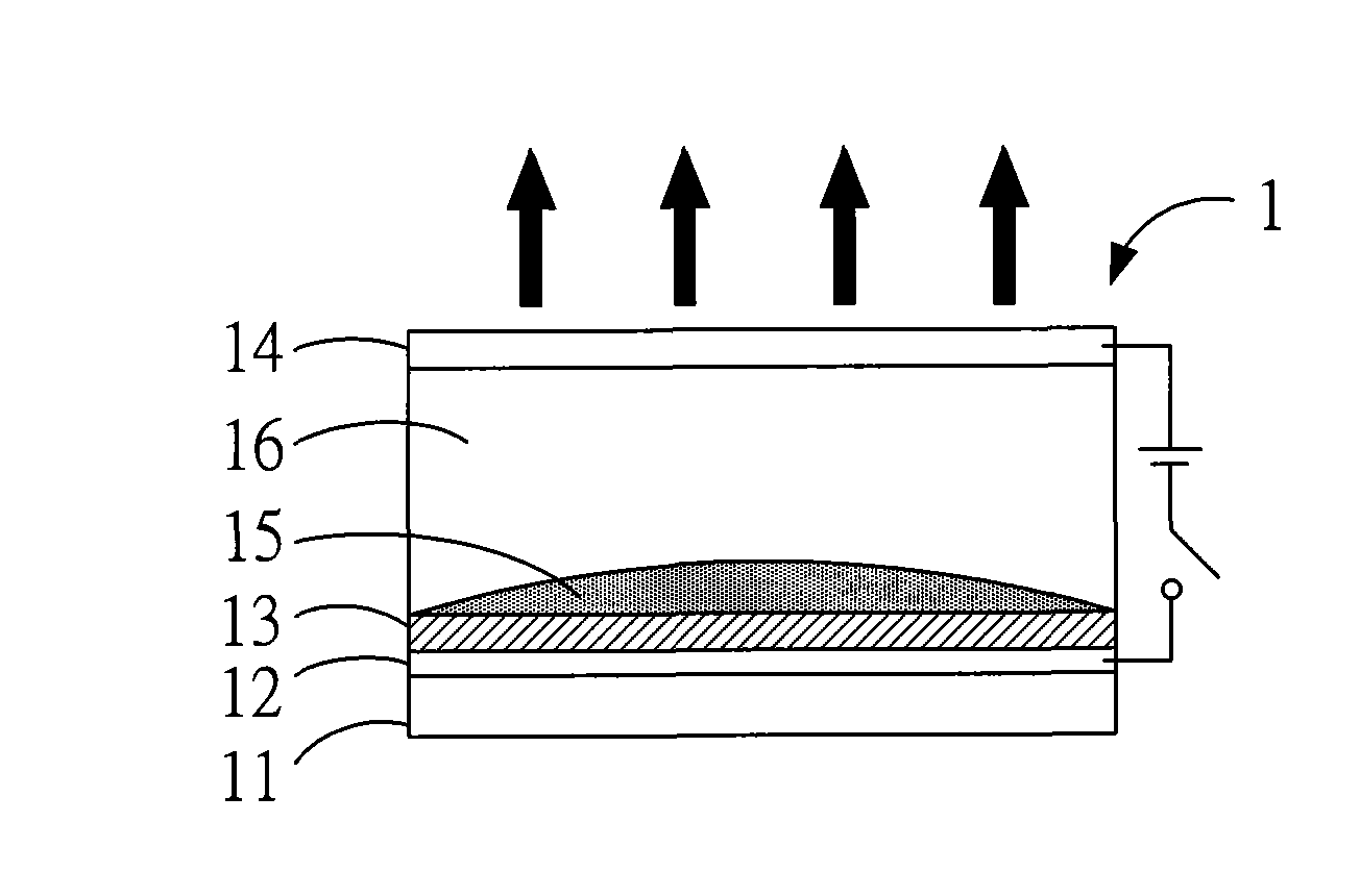
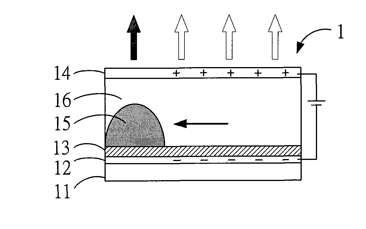
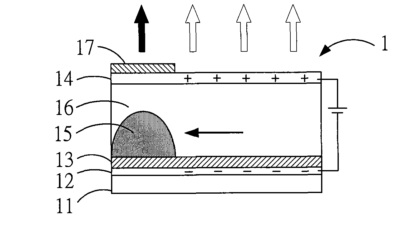
[0021] The present invention discloses a pixel structure 2 and a display device 100 comprising a plurality of pixel structures 2, wherein each pixel structure is as follows figure 2 and image 3 shown, the display device 100 please refer to Figure 4 shown. figure 2 It shows that the pixel structure of the present invention is in a state where no voltage is applied, image 3 Shown is the pixel structure of the present invention in a state of voltage application. The pixel structure 2 includes a first substrate 31 and a second substrate 40, the first substrate 31 is a transparent substrate as the light-emitting surface of the pixel structure 2, the second substrate 40 is an opaque substrate and is connected to the first substrate 31 relative settings. A layer of light-blocking layer 33 is disposed on the first substrate 31, and defines a light-transmitting area 331 (the white area in the light-blocking layer 33 as shown in the figure) and an opaque area 332 (the light-blo...


PUM


Abstract

The invention provides a pixel structure for a displaying device and the displaying device, wherein the pixel structure uses a light entering from the outside of the displaying device as a light source. The pixel structure comprises a first substrate, a light barrier layer, an active element and a moveable light shielding layer, wherein the light barrier layer is arranged on the first substrate and provided with a transparent area and a lightproof area; the active element is arranged in the lightproof area of the light barrier layer and has a first state and a second state; and the moveable light shielding layer is arranged on the light barrier layer and the active element. When the active element is in the first state, the moveable light shielding layer properly shields the transparent area so as to prevent the light from emitting out from the first substrate; and when the active element is in the second state, the moveable light shielding layer is driven to allow the light ray to passes through the transparent area and to be projected out from the first substrate.

Description

technical field [0001] The present invention relates to a display device; in particular, to a pixel structure applied to an electrowetting display device, and an electrowetting display device using the pixel structure. Background technique [0002] With the rapid development of science and technology, various portable electronic devices, such as mobile phones, personal digital assistants (PDA), digital cameras, digital video cameras, etc., bring great convenience to human life, and their specifications and functions are becoming more and more diversification. Among them, display technologies for portable electronic devices are constantly being developed to meet various demands. [0003] Since the portable electronic device emphasizes small size and light weight for portability, the portable electronic device must also consider power saving to prolong the battery life and avoid the trouble of frequent charging. Among them, the reflective display using external ambient light...

Claims


Application Information

Patent Timeline
Patent Type & Authority Applications(China)
IPC IPC(8): G02B26/02
Inventor 庄凯丞
Owner E INK HLDG INC
Why Eureka
Try Eureka