Compound for photoresist, photoresist solution, and etching method using the photoresist solution

A photoresist and compound technology, applied in chemical instruments and methods, complex metal compounds of azo dyes, photosensitive materials used in optomechanical equipment, etc., can solve problems such as increasing processes

Inactive Publication Date: 2010-03-17
FUJIFILM CORP
View PDF52 Cites 10 Cited by
  • Summary
  • Abstract
  • Description
  • Claims
  • Application Information

AI Technical Summary

Problems solved by technology

[0009] However, in the photolithography method using a conventional photoresist solution containing a photosensitive compound, a development step is necessary after pattern exposure, and as a result, only this part of the step is increased.

Method used


Image

  • Compound for photoresist, photoresist solution, and etching method using the photoresist solution
  • Compound for photoresist, photoresist solution, and etching method using the photoresist solution
  • Compound for photoresist, photoresist solution, and etching method using the photoresist solution

Examples


Embodiment 1

[0310] Formation of photoresist film

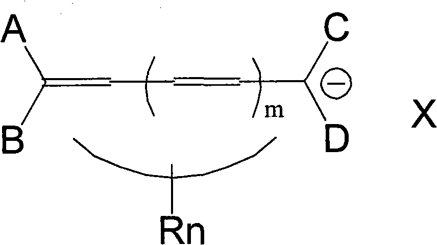
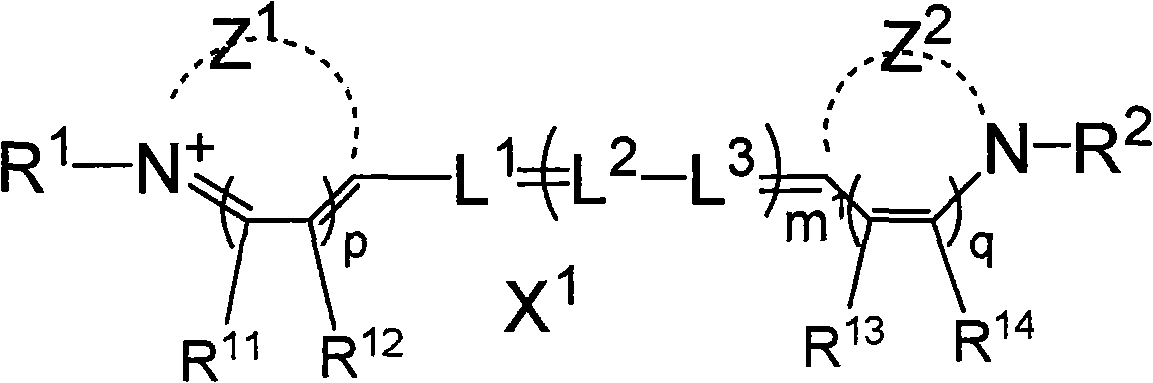
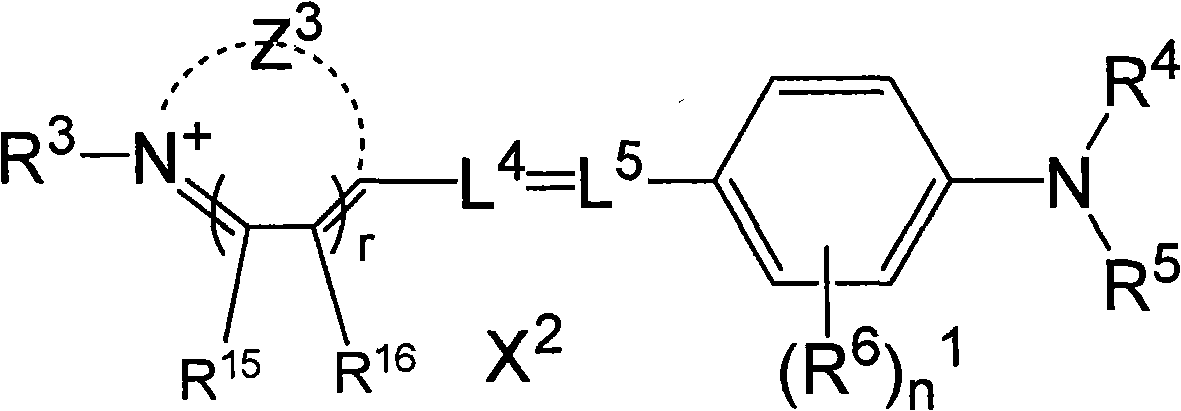
[0311] Dissolve 2 g of oxonol dye (example compound (II)-5, λmax of film: 378 nm, thermal decomposition temperature: 216° C.) in 100 ml of tetrafluoropropanol (TFP), and spin-coat it on a disk-shaped silicon substrate ( A coating film was formed on a thickness of 0.6 mm, an outer diameter of 120 mm, and an inner diameter of 15 mm. Spin coating is carried out as follows: the coating liquid is dispersed on the inner periphery of the substrate with the rotation speed of 500 rpm at the start of coating and 100 rpm at the end of coating, and the spin coating speed is gradually increased to 2200 rpm to make the coating film dry. The thickness of the formed coating film was 100 nm.

[0312] The silicon substrate on which the coating film was formed was set in NEO500 (wavelength: 405 nm, NA: 0.65) manufactured by Palos Technology Co., Ltd., and laser light was irradiated toward the coating film surface. The laser irradiation conditions are as ...

Embodiment 2

[0317] Bump formation

[0318] The silicon substrate treated in Example 1 was subjected to RIE etching from the side where the coating film was formed under the following conditions, and then the coating film was removed using ethanol as a stripping solution. It was confirmed with the naked eye that fine unevenness was formed on the coating film-removed surface of the silicon substrate surface. From this result, it is clear that the coating film treated in Example 1 functions as an etching mask.

[0319] Etching gas: SF 6 +CHF 3 (1:1)

[0320] Etching depth: 50nm

Embodiment 3~14

[0322] Except for using the exemplary compounds shown in Table 2 below as oxonol dyes, the same procedure as in Example 1 was carried out, and laser light was irradiated on the surface of the coating film. pit.

[0323] 【table 3】

[0324]


PUM

PropertyMeasurementUnit
thermal decomposition temperatureaaaaaaaaaa

Abstract

Disclosed is a compound for a photoresist, which is selected from the group consisting of a compound having an oxonol dye skeleton, a cyanine dye, a styryl dye, a compound having a merocyanine dye skeleton, a compound having a phthalocyanine dye skeleton, an azo compound and a complex compound of an azo compound with a metal ion. Also disclosed is a photoresist solution comprising at least one kind of the above-mentioned compound. Further disclosed is a method for etching a surface of interest by using the photoresist solution.

Description

[0001] Cross-references to related applications [0002] This application requires Japanese Patent Application No. 2007-054289 filed on March 5, 2007, Japanese Patent Application No. 2007-196756 filed on July 27, 2007, and Japanese Patent Application No. 2007-212149 filed on August 16, 2007 , Japanese Patent Application No. 2007-267664 filed on October 15, 2007, Japanese Patent Application No. 2007-267665 filed on October 15, 2007, Japanese Patent Application No. 2008-047243 filed on February 28, 2008, 2008 Japanese Patent Application No. 2008-047127 filed on February 28, 2008, Japanese Patent Application No. 2008-047130 filed on February 28, 2008, Japanese Patent Application No. 2008-047237 filed on February 28, 2008, 2008 February Priority of Japanese Patent Application No. 2008-047238 filed on March 28, and all the descriptions thereof are hereby specifically cited as disclosure content. technical field [0003] The present invention relates to a photoresist compound and a...

Claims


Application Information

Patent Timeline
Patent Type & Authority Applications(China)
IPC IPC(8): C09B23/00C09B29/48C09B45/14C09B45/18C09B45/20C09B45/48C09B47/12C09B47/18C09B47/20G03F7/004
CPCC09B29/337C09B23/0016C09B29/083C09B29/12C09B47/20C09B23/04C09B29/0037C09B69/04C09B29/081C09B23/086C09B23/0008C09B47/18C09B29/366C09B23/0091C09B23/0066C09B29/3652C09B29/3673C09B23/083G03F7/36G03F7/091C09B29/0081C09B29/0066C09B29/338C09B23/102C09B47/22C09B47/24C09B29/3634C09B29/0033C09B23/005C09B29/0092C09B23/06C09B23/107C09B29/004C09B29/0048C09B29/0088C09B29/0803C09B29/26C09B29/325C09B29/3604C09B29/3608C09B47/14C09B47/26C09B69/06C09B45/20C09B47/12G03F7/0045
Inventor 渡边哲也宇佐美由久
Owner FUJIFILM CORP
Why Eureka
Try Eureka