

Method for transferring thin film to substrate
A technology for substrates and films, which is applied in the field of transferring single-layer films from temporary surfaces to touch-sensitive surfaces, which can solve the problems of high cost, difficulty in driving lines and sensing lines, etc.
- Summary
- Abstract
- Description
- Claims
- Application Information
AI Technical Summary
Problems solved by technology
Method used
Image


Examples
Embodiment Construction
[0029] In the following description of the preferred embodiments, reference is made to the accompanying drawings, which form a part hereof, and in which are shown by way of illustration specific embodiments in which the invention may be practiced. It is to be understood that other embodiments may be utilized and structural changes may be made without departing from the scope of the preferred embodiments of the present invention.
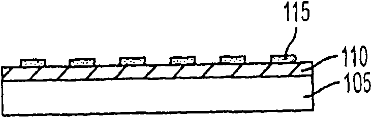
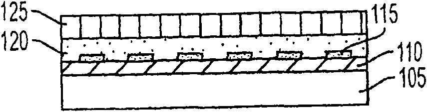
[0030] The present invention relates to the transfer of single-layer thin films of conductive materials to substrates used in devices such as touch sensor panels. In some embodiments, transfer can be accomplished by patterning a single layer of conductive material on one side of a transfer substrate and then transferring the patterned material from the transfer substrate to a target substrate. Such an approach advantageously allows the transfer of the patterned material to any target substrate, which may be one that cannot withstand standard manufact...
PUM
 Abstract
Description
Claims
Application Information