Vector modulation error compensation method based on analog base band correction

An Error Compensation, Analog Baseband Technology

Active Publication Date: 2012-07-04
CHINA ELECTRONIS TECH INSTR CO LTD
View PDF0 Cites 0 Cited by
  • Summary
  • Abstract
  • Description
  • Claims
  • Application Information

AI Technical Summary

Problems solved by technology

Its disadvantage is that the method of vector modulator with radio frequency phase shifter requires the design of a dedicated vector modulator, and this type of modulator is often produced by each large company or entrusted to a third party, and it is difficult to buy in the component market , and the special production of special vector modulators will inevitably require a lot of manpower and material resources
Its disadvantage is that the method of digital baseband correction lacks flexibility and can only be applied in the stage of digital baseband signal generation, and cannot correct the already formed analog baseband signal
For example, in the field of vector signal generation, it is often necessary to provide the function of external baseband signal input modulation. In this case, the method of digital baseband correction cannot be used.

Method used


Image

  • Vector modulation error compensation method based on analog base band correction
  • Vector modulation error compensation method based on analog base band correction
  • Vector modulation error compensation method based on analog base band correction

Examples


Embodiment Construction

[0025] The present invention will be described in further detail below in conjunction with the accompanying drawings.

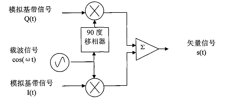
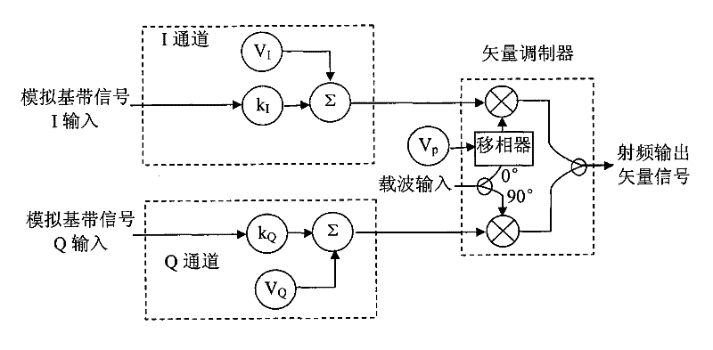
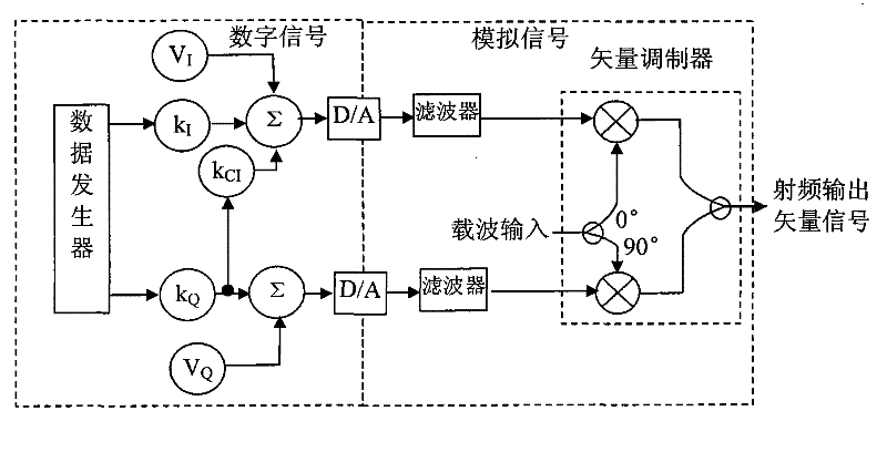
[0026] Such as Figure 4 The principle schematic diagram of the technical solution of the present invention shown, the vector modulator input signal is respectively: analog baseband signal I (t) and Q (t), carrier signal cos (ω t), vector modulator output signal is vector signal s (t ). To condition the input baseband signal, I(t) and Q(t) are input to the baseband channel circuit and then to the vector modulator. The relationship between input and output signals can be expressed as Equation 3:

[0027] s(t)=(V I +k I (I(t)+k CI Q(t)))cos(ωt)+(V Q +k Q k CQ Q(t))cos(ωt-π / 2) (3)

[0028] In Equation 3, V I and V Q Is the baseband bias voltage signal, used to compensate the carrier leakage; k I and k Q is the channel gain coefficient, which is used to compensate the I / Q amplitude balance error; k CI and k CQ is the quadrature phase error compensa...


PUM


Abstract

Disclosed is a vector modulation error compensation method based on analog base band correction. The method belongs to the testing technical field and is characterized by comprising following steps: 1, introducing a component for correcting phase included angles via a parameter KCI and a parameter KCQ, calculating the KCI and the KCQ according to a phase included angle theta of an in-phase component and an orthogonal component, obtaining the KCI equal to -ctg theta and the KCQ equal to 1 / sin theta; 2, enabling inputted analog base band signals to be zero, enabling kI and kQ to be equal, minimizing the magnitude of a carrier signal by properly adjusting values of VI and VQ; 3, enabling the magnitudes of the inputted analog base band signals to be equal, enabling the magnitudes of components of a vector signal to be equal by properly adjusting values of KI and KQ; 4, repeating the step 2 and the step 3 until error modulation of the vector signal meets design requirements. The method can properly correct the analog base band signals by means of introducing a correction vector relevant to a base band signal Q to a base band signal I according to the basic principle of vector signal combination, thereby substantially reducing vector modulation errors and improving quality of output signals of a vector modulator.

Description

technical field [0001] The invention relates to the technical field of testing, in particular to a vector modulation error compensation method based on analog baseband correction. Background technique [0002] Vector modulator principle such as figure 1 As shown, the digital modulation signal (vector signal) s(t) output by the vector modulator can be expressed as formula 1: [0003] s(t)=I(t)cos(ωt)+Q(t)cos(ωt-π / 2)=I(t)cos(ωt)+Q(t)sin(ωt) (1) [0004] In formula 1, I(t) and Q(t) are both analog baseband signals, cos(ωt) is the carrier signal, I(t)cos(ωt) is called the in-phase (in_phase) component, Q(t)sin(ωt ) are called quadrature components. [0005] In practical applications, due to the quadrature phase error, IQ amplitude balance error, and carrier leakage of the vector modulator and the baseband channel driving the vector modulator, the actual s(t) can be expressed as Equation 2: [0006] s(t)=(C I +I(t))cos(ωt)+(C Q +kQ(t))cos(ωωt-θ) (2) [0007] In formula 2, ...

Claims


Application Information

Patent Timeline
Patent Type & Authority Patents(China)
IPC IPC(8): H03C3/04H04L25/06
Inventor 盛振旗樊晓腾刘亮赵立新秦伟
Owner CHINA ELECTRONIS TECH INSTR CO LTD
Why Eureka
Try Eureka