Method for reducing current on bonded leads of power supply pads of chip
A technology of power supply pads and bonding wires, applied in circuits, electrical components, electrical solid devices, etc., can solve problems such as excessive current, and achieve the effects of easier implementation, reduced noise, and reduced current
- Summary
- Abstract
- Description
- Claims
- Application Information
AI Technical Summary
Problems solved by technology
Method used
Image

Examples
Embodiment Construction
[0017] The present invention will be further described in detail below in conjunction with the accompanying drawings and specific embodiments.
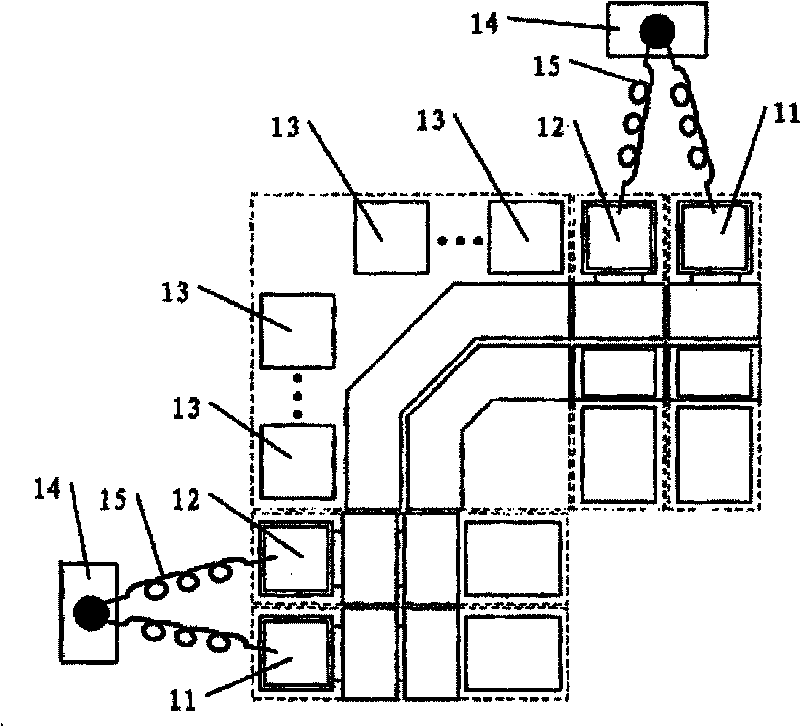
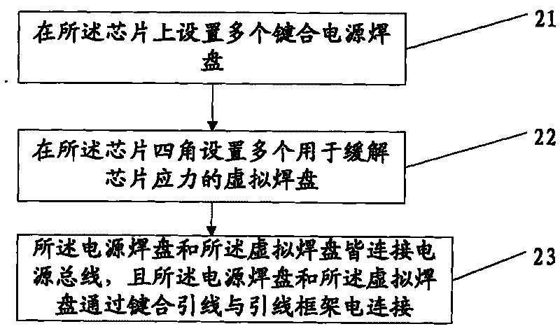
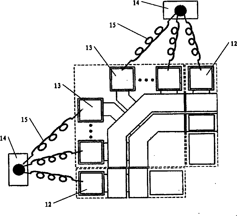
[0018] First, please refer to figure 2 , figure 2 It is a schematic flow chart of a method for reducing the current on the bonding wire of the chip power supply pad in the present invention, from figure 2 It can be seen that the present invention includes the following steps: Step 21: set a plurality of power supply pads on the chip, and the power supply pads are rectangular, octagonal or circular; Step 22: set a plurality of power pads at the four corners of the chip A dummy pad for alleviating chip stress, the dummy pad is rectangular, octagonal or circular; step 23: both the power pad and the dummy pad are connected to the power bus, and the power pad and The dummy pad is electrically connected to the lead frame through a bonding wire, the diameter of the bonding wire is in the range of 25 μm to 75 μm, and the power pad and th...
PUM
 Abstract
Description
Claims
Application Information
 - R&D Engineer
- R&D Manager
- IP Professional
- Industry Leading Data Capabilities
- Powerful AI technology
- Patent DNA Extraction
Browse by: Latest US Patents, China's latest patents, Technical Efficacy Thesaurus, Application Domain, Technology Topic.
© 2024 PatSnap. All rights reserved.Legal|Privacy policy|Modern Slavery Act Transparency Statement|Sitemap