Display panel

A technology for display panels and array substrates, applied in nonlinear optics, instruments, optics, etc., can solve problems such as light leakage, electric field interference, and disordered arrangement of liquid crystal molecules 132, so as to reduce the degree of confusion, reduce electric field interference, and achieve better display quality. Effect

Active Publication Date: 2011-05-04
AU OPTRONICS CORP
View PDF4 Cites 0 Cited by
  • Summary
  • Abstract
  • Description
  • Claims
  • Application Information

AI Technical Summary

Problems solved by technology

In particular, when the distance P1 between two adjacent stay wires 152 in the stay wire group 150 is very small, or the distance P2 between adjacent sections 152a of a stay wire 152 that is continuously bent (meandering) is very small, they will be adjacent to each other here. An electric field interference occurs between two pull wires 152 or between two adjacent segments 152a, which causes the arrangement of the liquid crystal molecules 132 to be more chaotic, resulting in light leakage
[0006] In particular, the black matrix 160 above the pull wire group 150 can only provide a certain degree of shading effect, and it is difficult to completely prevent the occurrence of light leakage
In addition, even if the liquid crystal display panel 100 is assembled into a liquid crystal display device, the frame or casing (not shown) around the liquid crystal display panel 100 also has a light-shielding effect, but light leakage will still occur due to structural design restrictions or assembly deviations. Affect display quality

Method used


Image

  • Display panel
  • Display panel
  • Display panel

Examples


Embodiment Construction

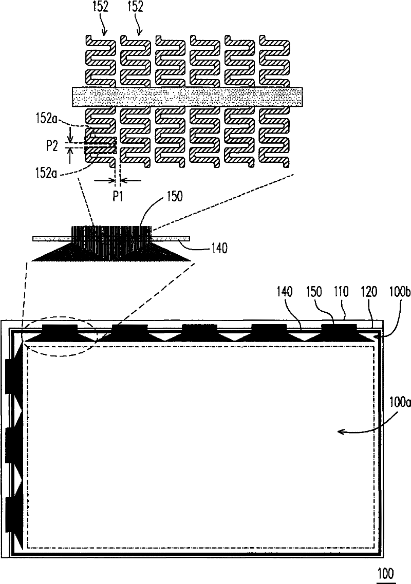
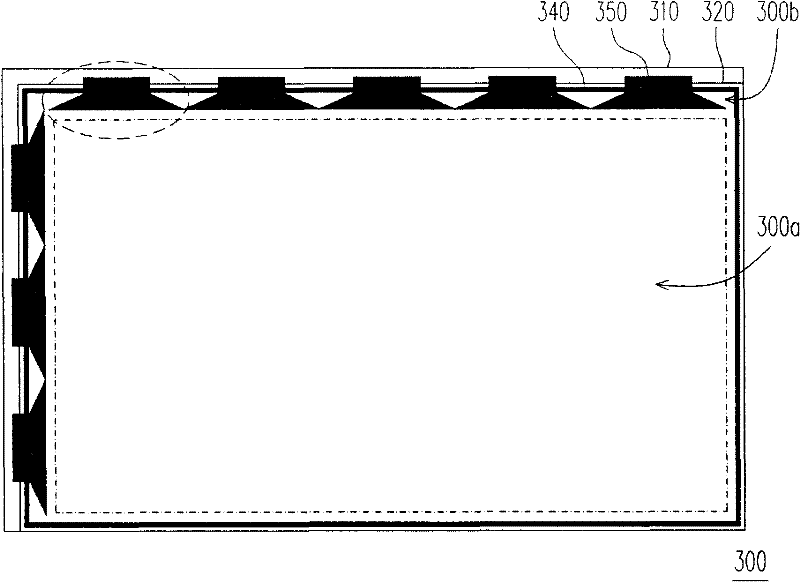
[0058] image 3 It is a top view of a display panel according to an embodiment of the present invention. Figure 4 for image 3 Partial cross-sectional view of the display panel.

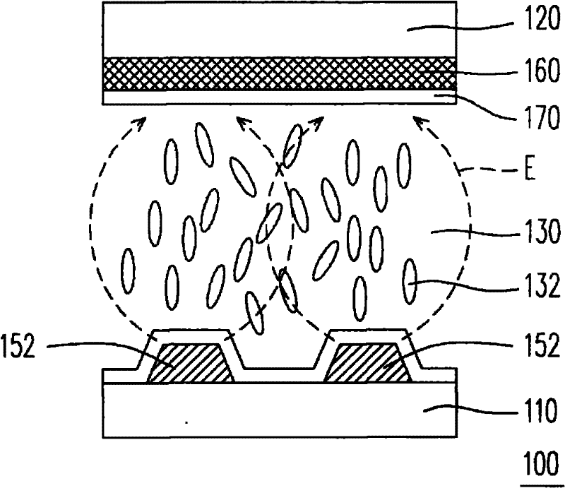
[0059] Such as image 3 and 4 As shown, the display panel 300 has an active area 300a and a peripheral circuit area 300b located around the active area 300a. The display panel 300 includes an active device array substrate 310 , an opposite substrate 320 , a display medium 330 and a sealant 340 . The active device array substrate 310 has a plurality of pixel structures 312 and a plurality of puller groups 350, wherein the pixel structures 312 are arranged in an array in the active area 300a, and the puller groups 350 are located in the peripheral circuit area 300b and are respectively electrically connected to their corresponding The pixel structure 312 . Further, the wire group 350 is electrically connected between the gate of the pixel structure 312 and an external gate driver, or is electric...


PUM


Abstract

The invention discloses a display panel, comprising a plurality of stay wire sets, wherein each stay wire set consists of a plurality of stay wires and the multiple stay wires extend along the same linear direction substantially; each stay wire is provided with a first part and a second part which are respectively arranged on opposite sides of sealant, the first part is arranged between the sealant and an active area of the display panel, and the shortest distance of any two adjacent stay wire sections in the first part is greater than that of any two adjacent stay wire sections in the secondpart. In addition, the shortest distance between any two adjacent stay wire sections in the first part is 15-35mu m. The design of the stay wire group can reduce electric field interference between adjacent stay wires and avoid light leak to improve the display quality.

Description

technical field [0001] The present invention relates to a display panel, and in particular to a display panel that reduces light leakage by changing the electric field distribution in the peripheral circuit area. Background technique [0002] In recent years, with the maturity of optoelectronic technology and semiconductor manufacturing technology, the flat panel display (FlatPanel Display, FPD) has been vigorously developed. Among them, the liquid crystal display is based on its low voltage operation, no radiation scattering, light weight and small size. Gradually replace the traditional cathode ray tube display and become the mainstream of display products in recent years. [0003] figure 1 It is a top view of a known liquid crystal display panel. Such as figure 1 As shown, the liquid crystal display panel 100 has an active area 100a and a peripheral circuit area 100b located on the periphery of the active area 100a. Pixel structures (not shown) arranged in an array ar...

Claims


Application Information

Patent Timeline
Patent Type & Authority Patents(China)
IPC IPC(8): G02F1/1345
CPCG02F1/1345G02F1/1339
Inventor 张峻桓傅建豪张君恺
Owner AU OPTRONICS CORP
Why Eureka
Try Eureka