Configurable on-chip testing module supporting encapsulation of different pins of chip

A technology of testing modules and pins, which is applied in the field of testing modules, can solve problems such as testing compatibility issues, and achieve the effects of wide testing range, flexible and targeted development, and strong versatility

Active Publication Date: 2010-05-12
苏州国芯科技股份有限公司
View PDF0 Cites 25 Cited by
  • Summary
  • Abstract
  • Description
  • Claims
  • Application Information

AI Technical Summary

Problems solved by technology

[0004] The invention provides a configurable on-chip test module that supports different pin packages of the chip, and aims to s

Method used


Image

  • Configurable on-chip testing module supporting encapsulation of different pins of chip
  • Configurable on-chip testing module supporting encapsulation of different pins of chip
  • Configurable on-chip testing module supporting encapsulation of different pins of chip

Examples


Embodiment

[0038] Embodiment: A configurable on-chip test module that supports packaging of different pins of the chip

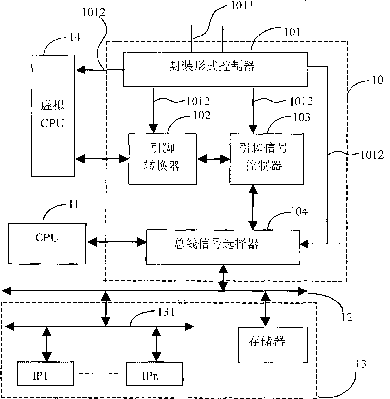
[0039] figure 1 It is a block diagram of the principle of the present invention. It can be seen from the figure that the chip is composed of CPU 11, bus 12, test module 10 and module group 13. Module group 13 includes memory, IP1~IPn application modules, and IP1~IPn application modules pass IP The bus 131 is connected to the bus 13 . The virtual CPU 14 is an incentive controller for reading and writing operations in the simulation test outside the chip.

[0040] The test module 10 will be described in detail below:

[0041] Such as figure 1 As shown, the test module 10 of the present invention is composed of a package type controller 101 , a pin converter 102 , a pin signal controller 103 and a bus signal selector 104 . The details of each component are as follows:

[0042] 1. Package type controller 101

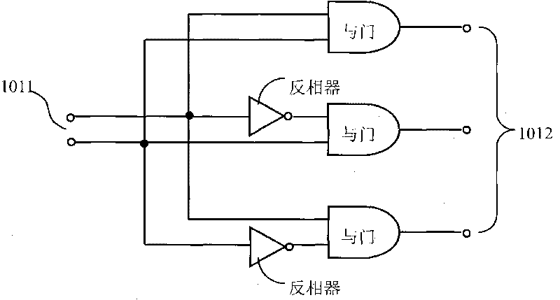
[0043] Package form controller 101 is provided by input p...


PUM


Abstract

The invention discloses a configurable on-chip testing module supporting the encapsulation of a chip through different pins, which consists of an encapsulation form controller (101), a pin converter (102), a pin signal controller (103) and a bus signal selector (104). The testing module can support the encapsulation form of the multifunctional chip that the different pins are adopted for different pieces of application. The configurable on-chip testing module supporting the encapsulation of the chip through the different pins is characterized in that: 1, the testing module is strong in universality and wide in testing range and can almost test all other functional modules except an internal CPU; 2, the testing module is less logical and can ignore influence on the area of the chip, thus the production cost of the chip is not increased; and 3, a virtual CPU (an excitation controller) adopted in testing is arranged outside the chip, thus the development on testing programs is more flexible and more relevant.

Description

technical field [0001] The invention relates to embedded chip technology, in particular to a test module in the embedded chip. The test module can be configured to support a multi-function chip with different pins (pins) for different applications. Background technique [0002] The current SOC (System on Chip, called system-on-chip or system-on-chip) technology is developing rapidly, and the product life cycle is shortened. It is often not economical to develop a chip for a certain application. More and more IC designers are more inclined to integrate more various functional modules on one chip, and then through subsequent market research and software development, the same chip can be used in different fields, thereby prolonging product survival cycle to maximize profits. The result of doing so will inevitably increase the number of pins in the chip design, but when such a chip design is applied to a specific field, it does not need so many pins, so when the same chip desi...

Claims


Application Information

Patent Timeline
IPC IPC(8): G01R31/28
Inventor 王宗宝肖佐楠郑茳林雄鑫
Owner 苏州国芯科技股份有限公司
Why Eureka
Try Eureka