Inductor and manufacturing method thereof

A production method and inductor technology, applied in the manufacture of inductors/transformers/magnets, transformer/inductor cores, inductors with magnetic cores, etc., can solve the problems of slow electrode oxidation, failure, product failure, etc., to prevent Effects of slow oxidation, increased coil area, and avoidance of adverse effects

Active Publication Date: 2012-03-28
SHENZHEN SUNLORD ELECTRONICS
View PDF0 Cites 0 Cited by
  • Summary
  • Abstract
  • Description
  • Claims
  • Application Information

AI Technical Summary

Problems solved by technology

Because the exposed electrodes will be slowly oxidized, and then fail to cause product failure, this large inductance design is rarely used in practice

Method used


Image

  • Inductor and manufacturing method thereof
  • Inductor and manufacturing method thereof
  • Inductor and manufacturing method thereof

Examples


Embodiment Construction

[0045] Embodiments of the present invention will be further described in detail below in conjunction with the accompanying drawings.

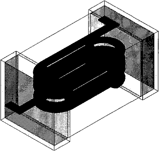
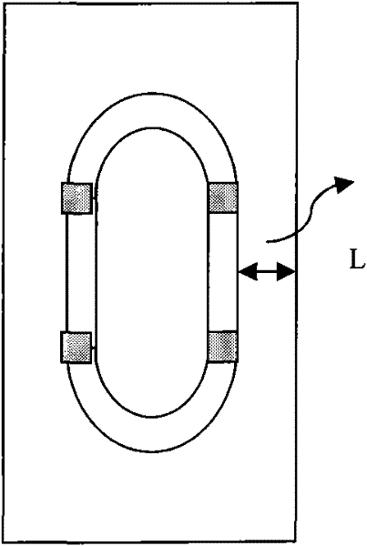
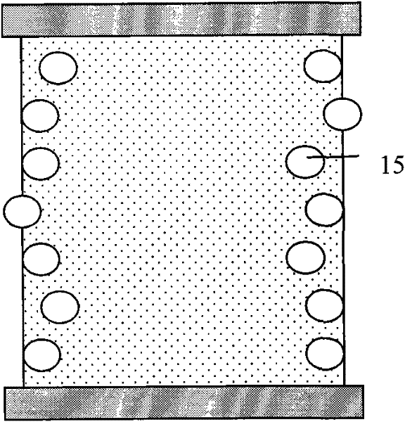
[0046] figure 2 , Figure 3a and Figure 3b A multilayer chip inductor 21 of an embodiment and its manufacturing method are shown, the inductor includes a magnet 10 and terminal electrodes 12, 13, a coil 15 is arranged inside the magnet, and the coil 15 is electrically connected to the Terminal electrodes 12, 13 (not shown), the edge of the coil 15 is close to the surface of the magnet 10, the surface of the magnet 10 is covered with a glass layer 11 except the end of the magnet, and the terminal electrodes are directly Combine with the end of the magnet.

[0047] See Figure 3a and Figure 3b According to the method of the present invention, an embodiment of manufacturing a multilayer chip inductor includes the following steps:

[0048] Step 1. Magnet preparation process

[0049] Known techniques can be used to form such Figure 3b Th...


PUM


Abstract

The invention discloses an inductor and a manufacturing method thereof. The inductor comprises a magnet and a terminal electrode, wherein the magnet is internally provided with a coil, and a coil electrode is connected with the terminal electrode; the edge of the coil approaches the surface of the magnet; a glass layer covers on the surface of the magnet except the end head of the magnet; and theterminal electrode is directly combined with the end head of the magnet. The manufacturing method comprises the following steps of: (a) magnet preparation: arranging the coil the edge of which approaches the surface of the magnet in the magnet; (b) forming the glass layer on the surface of the magnet except the end head of the magnet; and (c) forming the terminal electrode on the end head of the magnet and connecting the terminal electrode with the coil. At the same time of increasing the area of the coil in the inductor and improving the inductance, the invention can improve the quality factor Q of the inductor and guarantee the reliability of the inductor.

Description

technical field [0001] The invention relates to electronic components, in particular to an inductor and a manufacturing method thereof. Background technique [0002] In recent years, with the wide application of electronic components, while paying attention to the performance of components, more attention has been paid to the reliability of components, especially the reliability of life. Figure 1a It is a three-dimensional perspective schematic diagram of a multilayer chip ceramic inductor, which contains coil electrodes inside. With the development trend of inductors with super large inductance, the inductance of large inductance products at this stage is far from meeting the actual needs, and further development of products with greater inductance is needed. According to the calculation formula of inductance: [0003] L=u 0 u e N α S / l [0004] On the premise that the component material Ue and the component size are fixed, in order to increase the inductance L, the c...

Claims


Application Information

Patent Timeline
Patent Type & Authority Patents(China)
IPC IPC(8): H01F27/30H01F27/24H01F41/02H01F17/04
Inventor 孙峰戴春雷包汉青伍检灿
Owner SHENZHEN SUNLORD ELECTRONICS
Why Eureka
Try Eureka