IC test device

A test device and test probe technology, applied in the direction of measurement device, electronic circuit test, measurement of electricity, etc., can solve problems such as poor test yield and failure of test probes to achieve good contact, and achieve the effect of avoiding test failures

Inactive Publication Date: 2010-06-09
KING YUAN ELECTRONICS
View PDF0 Cites 10 Cited by
  • Summary
  • Abstract
  • Description
  • Claims
  • Application Information

AI Technical Summary

Problems solved by technology

However, in this multi-slot design test machine, the coplanarity between the slots and between the slots and the base is very important; if the coplanarity is not good, the test probe and the to-be The test IC w...

Method used


Image

  • IC test device
  • IC test device
  • IC test device

Examples


Embodiment Construction

[0030] Since the present invention provides an IC testing device, the principle of testing integrated circuit components used therein has been understood by those skilled in the art, so it will not be fully described in the following description. At the same time, the drawings compared below are schematic representations related to the features of the present invention, and are not and need not be completely drawn according to the actual situation and described in advance.

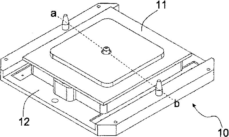
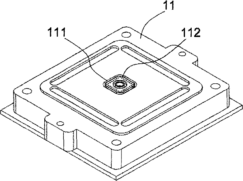
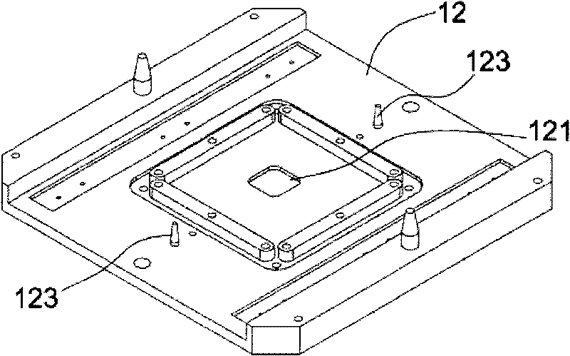
[0031] Please refer to figure 1 , is a schematic diagram of the IC testing device 10 of the first preferred embodiment provided by the present invention. The IC testing device 10 for testing after IC packaging mainly includes a top cover 11 (contact blade) and a base 12 (socket) assembled with each other. In a preferred implementation state, the IC testing device 10 is used for packaging and testing (CLCC, Ceramic Leaded Chip Package) of ceramic leaded chip carriers in image sensors.

[0032] Please cont...


PUM


Abstract

The invention relates to an IC test device which is used for testing the encapsulated IC. The IC test device mainly comprises an upper cover plate and a base which match each other. The invention is characterized in that a through hole is contained in the upper cover plate, a plurality of test probes are arranged near the through hole and used for contacting the IC, and a test spring is contained in each test probe. In addition, at least one bearing seat corresponding to the through hole in the upper cover plate is contained in the base and used for bearing the IC. At least one bearing spring is arranged between the lower part of the bearing seat and the base, the distance between the through hole and the bearing seat is smaller than the thickness of the encapsulated IC, and the coefficient of the elasticity of the bearing spring is greater than the sum of the coefficients of the elasticity of the plurality of test springs.

Description

technical field [0001] The invention relates to an IC testing device, in particular to a testing device applied to IC packaging. Background technique [0002] At present, some test machines used for testing IC packages use test probes to contact the packaged ICs to measure whether the packaged ICs meet the specifications. The design principle of the test IC packaging machine is that the contact between the IC and the test probe is that after the upper cover and the base are in contact, there is a gap between the IC bearing surface of the upper cover and the bearing surface of the base. The distance is preset as the thickness of the IC to be tested, so that the test probes arranged on the upper cover are in contact with the IC to be tested to achieve the purpose of testing the IC. [0003] However, in the use of this known test device, the thickness of the IC after packaging often has errors. When testing, if the thickness of the package is greater than the preset value, it ...

Claims


Application Information

Patent Timeline
IPC IPC(8): G01R31/28G01R1/073
Inventor 黎孟达
Owner KING YUAN ELECTRONICS
Why Eureka
Try Eureka