MOS (Metal Oxide Semiconductor) transistor and fabricating method thereof

A technology of a MOS transistor and a manufacturing method, which is applied to the field of MOS transistors and their manufacturing, can solve the problems of control and matching affecting the threshold voltage of the transistor, and enhance the diffusion of impurities, and achieve the effects of suppressing transients and enhancing the diffusion effect.

Active Publication Date: 2010-06-16
SEMICON MFG INT (SHANGHAI) CORP
View PDF1 Cites 14 Cited by
  • Summary
  • Abstract
  • Description
  • Claims
  • Application Information

AI Technical Summary

Problems solved by technology

In the existing process for forming MOS transistors, it is usually necessary to implant ions in the channel to adjust the threshold voltage of the transistor. The implanted ions are usually boron ions for nMOS transistors, and phosphorus ions for pMOS transistors. The carbon in the above technical solution The step of ion implantation fails to suppress the defects caused by the process before the formation of the source / drain extension region such as the above-mentioned channel implantation and gate oxide layer growth to form the gate dielectric layer. Due to the existence of these defects and the subsequent low temperature process The process will lead to enhanced diffusion of impurities in the channel region, affecting the control and matching of the threshold voltage of the transistor

Method used


Image

  • MOS (Metal Oxide Semiconductor) transistor and fabricating method thereof
  • MOS (Metal Oxide Semiconductor) transistor and fabricating method thereof
  • MOS (Metal Oxide Semiconductor) transistor and fabricating method thereof

Examples


Embodiment Construction

[0035] Below by describing specific embodiment in detail according to accompanying drawing, above-mentioned object and advantage of the present invention will be clearer:

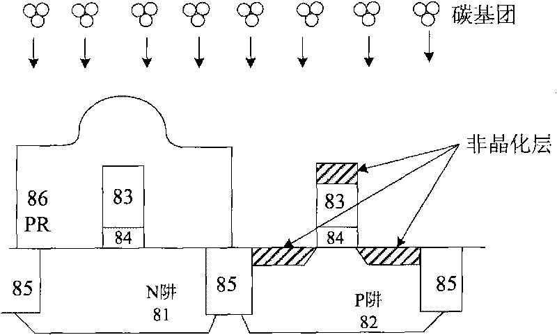
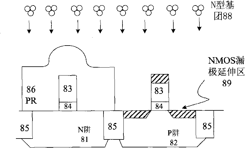
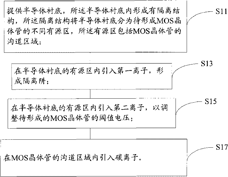
[0036] The present invention firstly provides a manufacturing method of a MOS transistor, please refer to figure 1 , including: performing step S11, providing a semiconductor substrate, an isolation structure is formed in the semiconductor substrate, and the isolation structure divides the semiconductor substrate into different active regions where MOS transistors are to be formed, and the active regions include MOS The channel region of the transistor; perform step S13, introduce the first ion in the active region of the semiconductor substrate to form an isolation well; perform step S15, introduce the second ion in the active region of the semiconductor substrate, to adjust the threshold voltage of the MOS transistor; execute step S17 to introduce carbon ions into the channel region of the MOS transistor...


PUM


Abstract

The invention provides an MOS (Metal Oxide Semiconductor) transistor and a fabricating method thereof. The fabricating method of the MOS transistor comprises the steps of: providing a semiconductor substrate, wherein an active area in the semiconductor substrate comprises a channel area of the MOS transistor; introducing a first ion in the active area of the semiconductor substrate to form an isolation well; introducing a second ion in the active area of the semiconductor substrate to adjust the threshold voltage of an MOS transistor to be formed; and introducing a carbon ion in the channel area of the MOS transistor, wherein the step of the introduction of the carbon ion is carried out before or after the introduction of the first ion, or before or after the introduction of the second ion. Accordingly, the invention also provides an MOS transistor fabricated by the fabricating method. By introducing the carbon ion in the channel area of the MOS transistor, the invention stops ions injected in the channel area of the MOS transistor later from diffusing in a subsequent process for forming a gate dielectric layer by oxidization, thereby achieving the aim of inhibiting the transient enhanced diffusion effect.

Description

technical field [0001] The invention relates to the technical field of semiconductors, in particular to a MOS transistor and a manufacturing method thereof. Background technique [0002] As the gate length of transistors continues to shrink, oxidation-enhanced diffusion (Oxidation-Enhanced Diffusion, OED) has become a key factor affecting the diffusion of boron and phosphorus ions. Due to the OED effect, transient enhanced diffusion effect (TED) is caused, and the transient The enhanced diffusion effect not only causes the short channel effect of the transistor, but also affects the channel mobility, junction capacitance and junction leakage current of the transistor. [0003] The prior art discloses a method of using implanted carbon clusters to form shallow junctions to control the diffusion of boron ions in the source and drain electrodes of transistors, and to form stress in the silicon substrate by implanting carbon clusters at a high dose. , see below for details Fig...

Claims


Application Information

Patent Timeline
IPC IPC(8): H01L21/8234H01L21/336H01L27/04H01L29/78
Inventor 赵猛
Owner SEMICON MFG INT (SHANGHAI) CORP
Why Eureka
Try Eureka