
A kind of ggnmos device and manufacturing method thereof

A manufacturing method and device technology, applied in the direction of semiconductor/solid-state device manufacturing, semiconductor devices, electrical components, etc., can solve the problems of increasing the device area, reducing the slope of the conduction curve, affecting the ESD discharge capability, etc., and reducing the P-well Concentration, Improved Trigger Effect, Good Trigger Effect

Active Publication Date: 2012-02-15
SHANGHAI HUAHONG GRACE SEMICON MFG CORP
View PDF0 Cites 0 Cited by
  • Summary
  • Abstract
  • Description
  • Claims
  • Application Information

AI Technical Summary

Problems solved by technology

However, an excessively long drain length not only increases the device area, but also reduces the slope of the conduction curve too much, which affects the ESD discharge capability.

Method used


Image

  • A kind of ggnmos device and manufacturing method thereof
  • A kind of ggnmos device and manufacturing method thereof
  • A kind of ggnmos device and manufacturing method thereof

Examples


Embodiment Construction

[0030] The manufacturing method of GGNMOS device described in the present invention, comprises the steps:

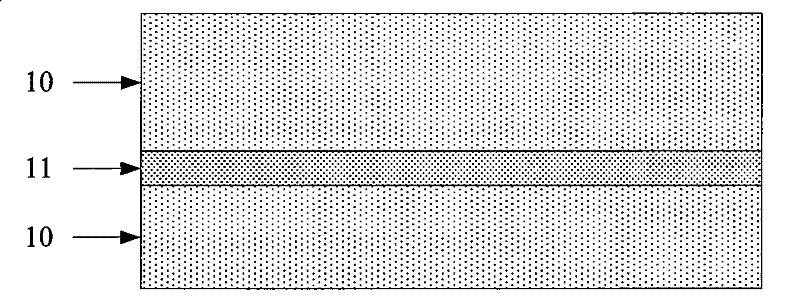
[0031] Step 1, see Figure 1a . N-type impurities are implanted on the P-type silicon substrate 10 by an ion implantation process to form a deep N well 11 . Commonly used N-type impurities are phosphorus, arsenic and antimony. Annealed in a high temperature furnace after ion implantation.

[0032] For example, the dose of ion-implanted phosphorus is 5×10 12 ions / cm 2 (ion per square centimeter) ~ 1.5×10 13 ions / cm 2 , the implantation energy is 1000keV-2000keV. The temperature of the high temperature furnace annealing is 1100° C. to 1200° C., and the time is 1 to 3 hours.

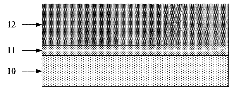
[0033] Step 2, see Figure 1b . P-type impurities are implanted on the P-type silicon substrate 10 by an ion implantation process, and the range of ion implantation is all silicon above the deep N well 11 , thereby forming a P well 12 on the deep N well 11 . Commonly used P-type impurities ...


PUM


Abstract

The invention discloses a GGNMOS device in a deep N well. Under the condition that all dimensions of the device remain unchanged, the channel resistance can be significantly increased to realize good triggering of the GGNMOS, and the device can be maintained in a smaller size range, saving energy. chip area. The core of the invention is to put the GGNMOS device in the deep N well, instead of making it on the P-type substrate like the conventional GGNMOS device. Its advantages are: 1. The out-diffusion of phosphorus atoms in the deep N-well compensates the boron atoms in part of the P-well, reduces the effective P-well concentration, increases the channel resistance, and improves the triggering effect of GGNMOS; 2. Because the deep N-well isolates The P well and P-type substrate reduce the flow cross-sectional area of ​​the source-drain current and further increase the channel resistance.

Description

technical field [0001] The invention relates to a semiconductor integrated circuit device, in particular to a MOS device. [0002] semiconductor manufacturing Background technique [0003] GGNMOS (gate-grounded NMOS, Gate-Grounded NMOS) is a basic element of an ESD (Electrostatic Discharge) circuit, and its electrostatic discharge capability determines the performance of an ESD circuit. The conventional GGNMOS process is formed by modifying the device structure on the basis of I / O NMOS, such as appropriately increasing the channel length, increasing the length of the drain terminal, and increasing ESD ion implantation, etc., in order to appropriately reduce the trigger voltage (Vt1, also known as primary breakdown voltage), adjust the sustain voltage (Vsp) and the slope of the conduction curve, and adjust the secondary breakdown voltage (Vt2) to be slightly greater than the trigger voltage. In order to effectively trigger the ESD device, in addition to reducing the trigger...

Claims


Application Information

Patent Timeline
Patent Type & Authority Patents(China)
IPC IPC(8): H01L29/78H01L21/336
Inventor 钱文生
Owner SHANGHAI HUAHONG GRACE SEMICON MFG CORP
Learn More