Electrostatic discharging protection device and protection method thereof

A technology of electrostatic discharge protection and cutting-edge discharge, which is applied in the direction of circuits, electrical components, electric solid devices, etc., and can solve problems such as interference, ESD entering the system, electronic components or electronic system failures, etc.

Inactive Publication Date: 2010-06-23
HOLTEK SEMICON
View PDF0 Cites 10 Cited by
  • Summary
  • Abstract
  • Description
  • Claims
  • Application Information

AI Technical Summary

Problems solved by technology

[0002] Electrostatic discharge (ESD, Electrostatic Discharge) is one of the main problems in the connection process of electronic equipment. It will cause many electronic components or electronic systems to fail, causing electronic equipment manufacturers to suffer a lot of losses.
In addition, multi-functionality and miniaturization have become the current design trend of handheld products. However, when these handheld products are required to provide multi-functions, their I / O ports will also increase, which will easily cause ESD to enter the system, and then interfere or damage the integration. circuit

Method used


Image

  • Electrostatic discharging protection device and protection method thereof
  • Electrostatic discharging protection device and protection method thereof
  • Electrostatic discharging protection device and protection method thereof

Examples


Embodiment Construction

[0053] The present invention will be fully understood by the following examples, so that those skilled in the art can complete it, but the implementation of the present invention should not be limited by the following examples.

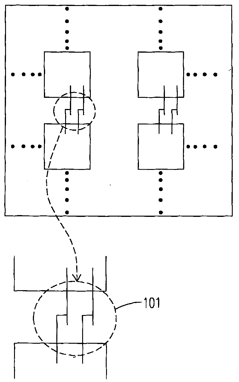
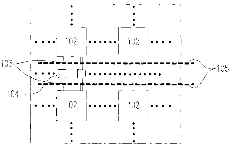
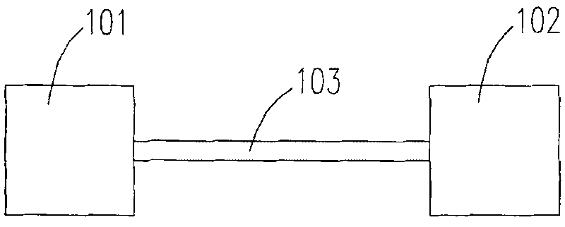
[0054]Please refer to FIG. 3(A), which is a schematic diagram of a wafer provided with the ESD protection device of the present invention. First, a first electrical connection pad 101 and a second electrical connection pad 102, and the first electrical connection pad and the second electrical connection pad are placed on any die in a wafer; wherein The first electrical connection pad and the second electrical connection pad are respectively a VDD terminal electrical connection pad and a VSS terminal electrical connection pad; a fuse 103 is used to connect the two electrical connection pads, and the process is completed. Device with ESD protection of the present invention.

[0055] Please refer to FIG. 3(B), which is a device with protection against E...


PUM


Abstract

The invention discloses an electrostatic discharging (ESD) protection device and a protection method thereof. A plurality of crystal particles are provided, each crystal particle is provided with a first electric connecting pad, the first electric connecting pad is electrically connected with a sealing ring which forms a border of the crystal particle, and a second electric connecting pad is electrically connected with a second electric connecting pad so as to achieve the effect of protecting the electrostatic discharging.

Description

technical field [0001] The invention relates to a device for protecting electrostatic discharge on a wafer and a protection method thereof, in particular to an ESD protection device and a protection method thereof. Background technique [0002] Electrostatic discharge (ESD, Electrostatic Discharge) is one of the main problems in the connection process of electronic equipment. It will cause many electronic components or electronic systems to fail, causing electronic equipment manufacturers to suffer a lot of losses. In addition, multi-functionality and miniaturization have become the current design trend of handheld products. However, when these handheld products are required to provide multi-functions, their I / O ports will also increase, which will easily cause ESD to enter the system, and then interfere or damage the integration. circuit. [0003] The reason for the destruction of ESD is that in addition to human factors, the electronic components themselves will also accu...

Claims


Application Information

Patent Timeline
Patent Type & Authority Applications(China)
IPC IPC(8): H01L23/60H01L21/00H01L21/66
Inventor 邓志辉
Owner HOLTEK SEMICON
Why Eureka
Try Eureka