High-voltage tolerance output buffer
An output buffer, high-voltage technology, applied in the direction of logic circuit connection/interface layout, logic circuit coupling/interface using field effect transistors, etc., to avoid instability and ensure normal operation.
- Summary
- Abstract
- Description
- Claims
- Application Information
AI Technical Summary
Problems solved by technology
Method used
Image
Examples
Embodiment Construction
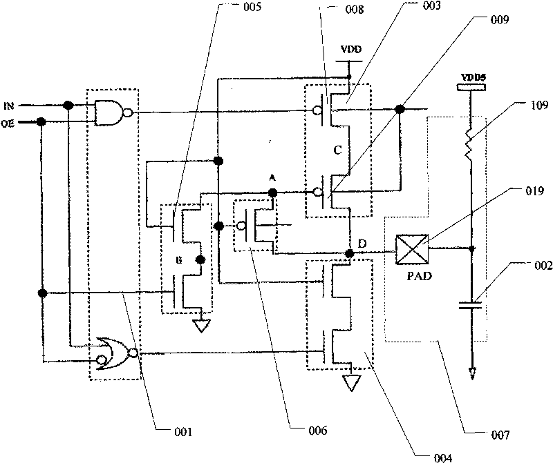
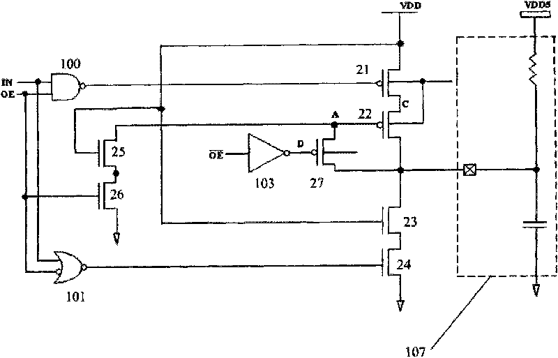
[0027] Please refer to figure 2 , figure 2It is the circuit diagram of the output buffer of the present invention that can withstand high voltage, it includes an input module, the input terminal is connected to the input signal (IN) and the output enable signal (OE), and includes a NAND gate 100 and a NOR gate 101, so The input terminals of the NAND gate 100 are IN and OE, and the input terminals of the NOR gate 101 are IN and OE; the pull-up module receives the first output signal of the input module, between the first voltage and the output point A high-impedance or low-impedance circuit is provided according to the received signal, the pull-up module includes a first transistor 21 and a second transistor 22, the gate of the first transistor 21 is connected to the output terminal of the NAND gate 100, The drain of the first transistor 21 is connected to the source of the second transistor 22, the first transistor 21 and the second transistor 22 are used for pull-up, and t...
PUM
 Abstract
Description
Claims
Application Information


