Supercharge Your Innovation With Domain-Expert AI Agents!

Active matrix type display device and driving method thereof

A display device and active matrix technology, applied in static indicators, nonlinear optics, instruments, etc., can solve problems such as uneven display, and achieve the effect of reducing uneven display

Inactive Publication Date: 2010-07-07
CASIO COMPUTER CO LTD
View PDF1 Cites 0 Cited by
  • Summary
  • Abstract
  • Description
  • Claims
  • Application Information

AI Technical Summary

Problems solved by technology

[0030] In the method disclosed in the above-mentioned JP Patent Application No. 2004-185006, it is impossible to deal with such inter-pixel parasitic capacitance 104, which occurs in the first written pixel. The problem of uneven display caused by potential fluctuations

Method used


Image

  • Active matrix type display device and driving method thereof
  • Active matrix type display device and driving method thereof
  • Active matrix type display device and driving method thereof

Examples


no. 1 Embodiment

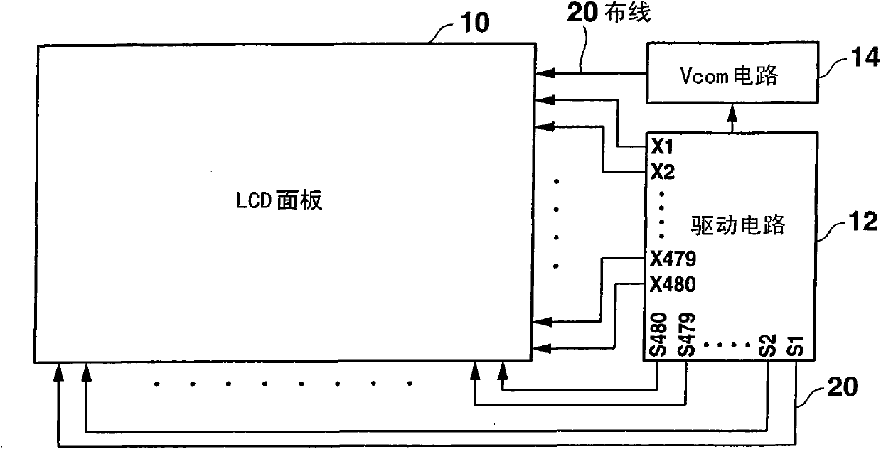
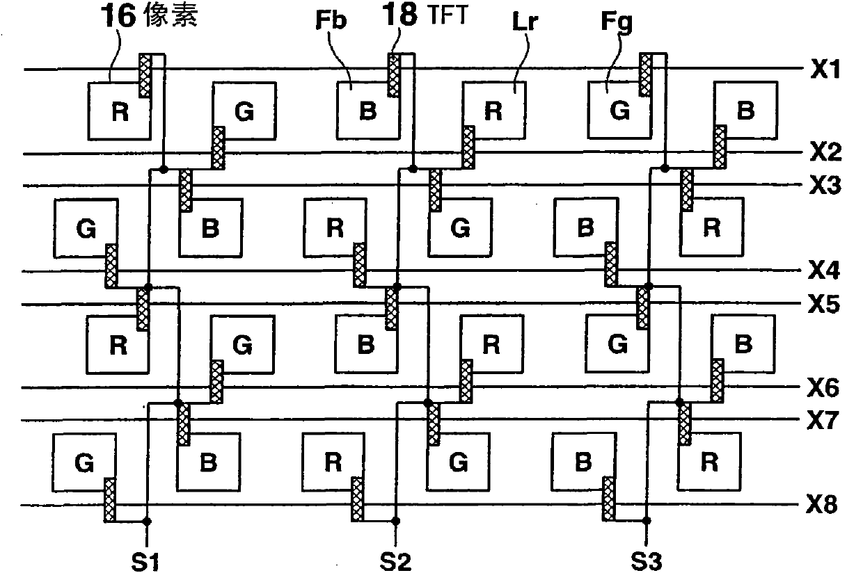
[0101] Figure 1A It is a schematic diagram showing the overall structure of the active matrix display device of the first embodiment of the present invention, Figure 1B for Figure 1A A schematic diagram of the pixel connection of the LCD panel in ;

[0102] That is, the active matrix type display device of this embodiment is like Figure 1A As shown, it is composed of a panel 10 provided with a plurality of pixel LCDs, a drive circuit 12 for driving and controlling each pixel of the LCD panel 10 , and a Vcom circuit 14 for applying a common voltage Vcom to the LCD panel 10 .

[0103] LCD panel 10 images Figure 1B As shown, a plurality of pixels are arranged in a matrix. In addition, a plurality of source lines S1 to S480 and a plurality of gate lines X1 to X480 are arranged to cross each other. In addition, each pixel is connected to one of the source lines and one of the gate lines through the TFT 18 which is a switching element. Here, each pixel is provided so that...

no. 2 Embodiment

[0147] Next, a second embodiment of the present invention will be described.

[0148] In this embodiment, the potential variation Vc caused by the inter-pixel parasitic capacitance Cpp is added to the previously written pixel potential and written, thereby canceling the potential variation Vc caused by the inter-pixel parasitic capacitance Cpp, and eliminating display failure. uniform.

[0149] Here, a case where the potential variation is corrected using the gamma circuit module 30 of the drive circuit 12 will be described. In addition, the case of a still image in which unevenness tends to be conspicuous will be described.

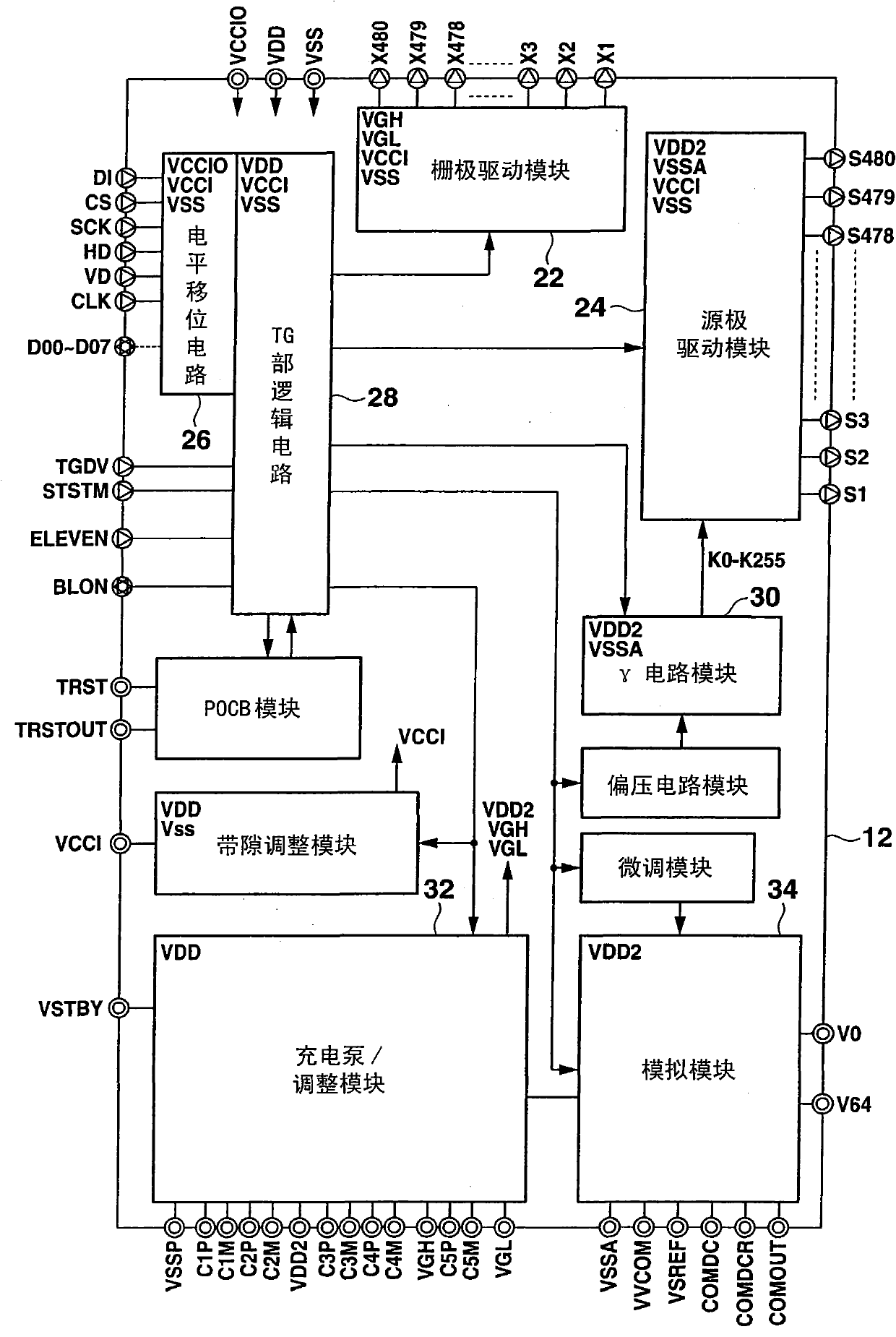
[0150] picture figure 2 As shown, the driver circuit 12 has a gamma circuit module 30 . Figure 5 It is a diagram showing the circuit configuration of the gamma circuit module 30 . As shown in the figure, the gamma circuit module 30 is composed of a gamma curve resistor 38 and a tap switch (hereinafter referred to as TAPSW) 40 . For the gamma curve ...


PUM


Abstract

An active matrix type display device in which one signal line is provided for every two pixels along a given direction and in which two pixels adjacent in the given direction on respective sides of one signal line share the signal line and are connected to respective different scanning lines, through switching elements. A scanning line driving circuit selects the plurality of scanning lines in turn, and a signal line driving circuit outputs signals according to information to be displayed to the plurality of signal lines. The scanning line driving circuit simultaneously selects two scanning lines corresponding to two pixels connected to different signal lines and adjacently disposed in the given direction and then selects only one scanning line corresponding to a pixel to be selected later out of the two pixels for only a prescribed period.

Description

[0001] The application for this invention is the result of an invention patent filed by the applicant "Casio Computer Corporation" to the State Intellectual Property Office on September 28, 2007 with the application number "200710199979X" and the invention name "Active Matrix Display Device and Driving Method". Divisional application. technical field [0002] The present invention relates to an active matrix display device and a driving method of a type in which one signal line is shared by two adjacent pixels. Background technique [0003] In recent years, active matrix display devices using thin film transistors (TFTs) as switching elements are being developed. [0004] This active matrix display device has a scanning line driver circuit (hereinafter referred to as a gate driver) that generates a scanning signal for sequentially scanning a plurality of pixels arranged in a matrix for each row. The operating frequency of the gate driver is lower than that of a signal line ...

Claims


Application Information

Patent Timeline
Patent Type & Authority Applications(China)
IPC IPC(8): G09G3/36G09G3/20
CPCG09G3/3648G09G2310/027G09G2320/0209G09G2320/0233G09G3/3677G09G2320/0673G09G3/3614G09G3/3696G09G2320/0276G09G2310/0278G09G2300/0426G02F1/133G09G3/20G09G3/36
Inventor 平山隆一
Owner CASIO COMPUTER CO LTD
Features
  • R&D
  • Intellectual Property
  • Life Sciences
  • Materials
  • Tech Scout
  • Unparalleled Data Quality
  • Higher Quality Content
  • 60% Fewer Hallucinations
Learn More