Multilayered wiring board and semiconductor device

A multi-layer wiring substrate and semiconductor technology, which is applied in semiconductor devices, semiconductor/solid-state device components, multi-layer circuit manufacturing, etc., can solve the problems of deformation of rigid parts, rigid flexible substrates cannot be installed with high reliability, etc.

Inactive Publication Date: 2010-07-21
SUMITOMO BAKELITE CO LTD
View PDF1 Cites 10 Cited by
  • Summary
  • Abstract
  • Description
  • Claims
  • Application Information

AI Technical Summary

Problems solved by technology

Therefore, the rigid portion is easily deformed by external factors such as heat, and as a result, the rigid-flex substrate cannot achieve high mounting reliability like the above-mentioned rigid substrate

Method used


Image

  • Multilayered wiring board and semiconductor device
  • Multilayered wiring board and semiconductor device
  • Multilayered wiring board and semiconductor device

Examples


no. 1 approach

[0035] First, a first embodiment of the present invention will be described.

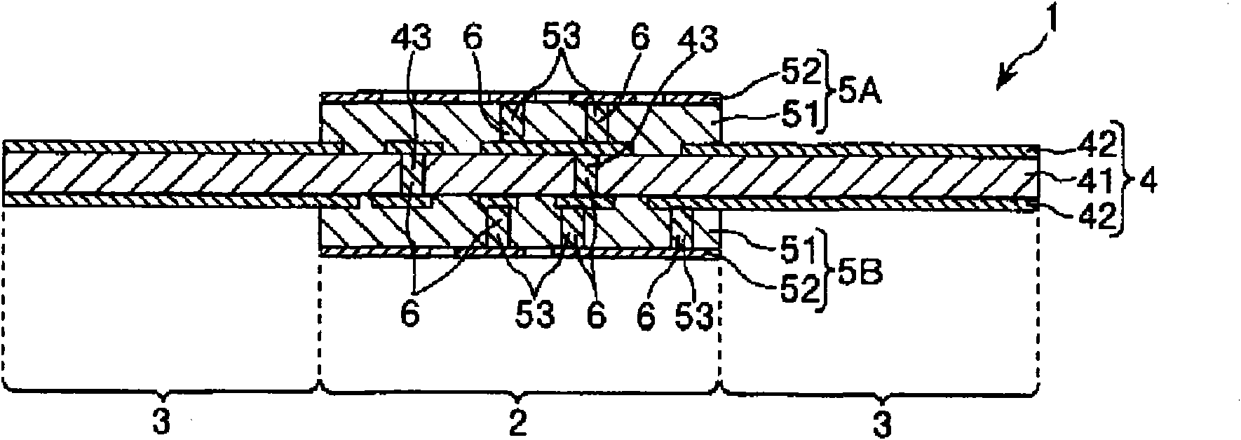
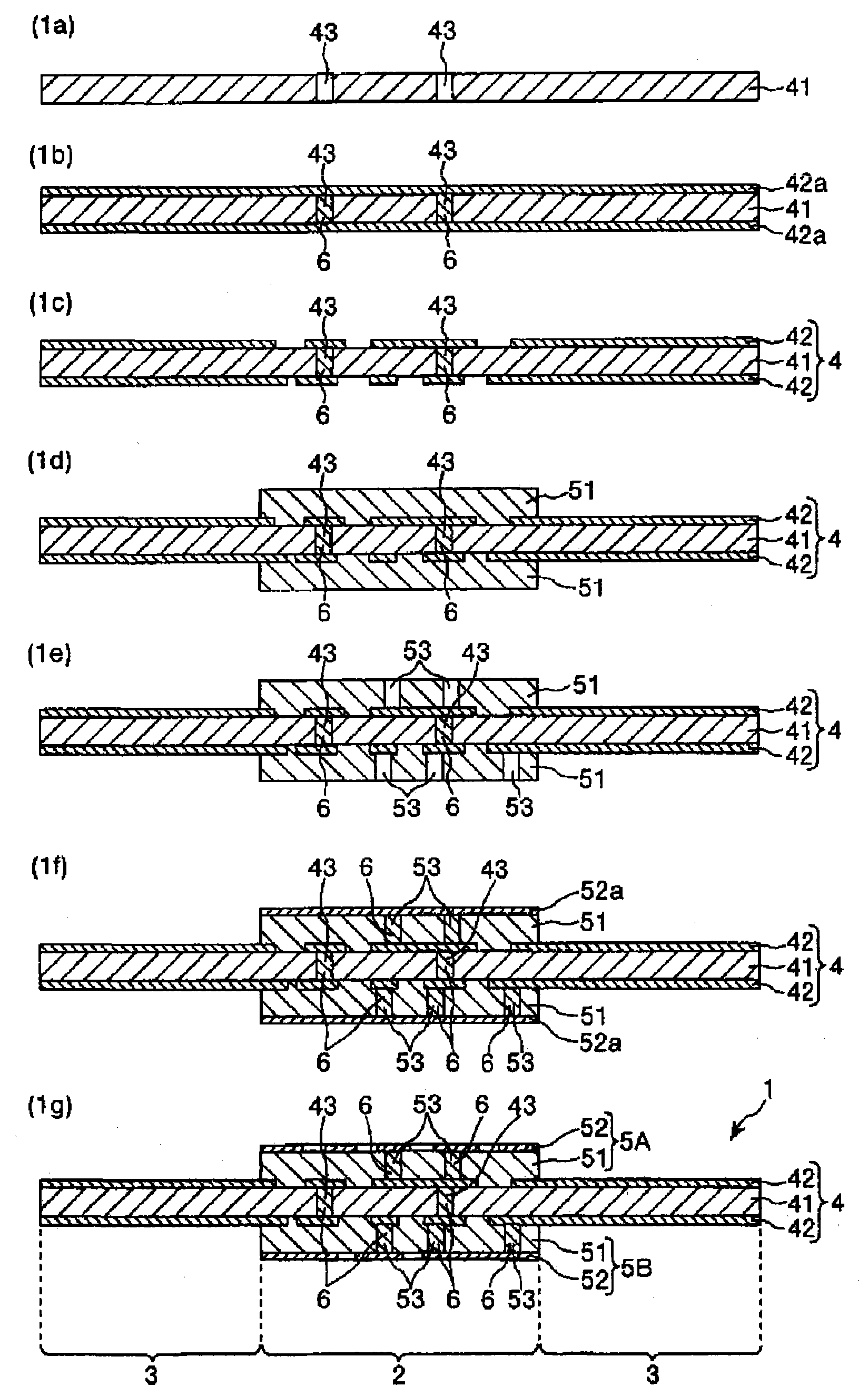
[0036] figure 1 It is a longitudinal sectional view showing the first embodiment of the multilayer wiring board of the present invention, figure 2 yes means figure 1 A vertical cross-sectional view of a preferred method of manufacturing a multilayer wiring substrate is shown, image 3 It is a longitudinal cross-sectional view showing the semiconductor device of this embodiment. In addition, for the convenience of explanation below, the figure 1 , figure 2 The upper side is referred to as "upper" or "upper", and the lower side is referred to as "lower" or "below".

[0037] like figure 1 As shown, the multilayer wiring substrate 1 has: a rigid part 2 having high rigidity; and a flexible part 3 having flexibility connected to both ends of the rigid part 2 .

[0038]

[0039] First, the rigid portion 2 will be described.

[0040] like figure 1 As shown, the rigid part 2 has high rigidity, a...

no. 2 approach

[0170] Next, a second embodiment of the present invention will be described.

[0171] Figure 4 is a longitudinal sectional view showing a second embodiment of the multilayer wiring board of the present invention, Figure 5 , Image 6 , Figure 7 yes means Figure 4 A vertical cross-sectional view of a preferred method of manufacturing the multilayer wiring board shown. In addition, in the following, for convenience of description, the upper side in the figure is called "upper" or "upper", and the lower side is called "lower" or "below".

[0172] Next, a second embodiment of the present invention will be described with reference to the drawings. However, differences from the above-mentioned embodiment will be mainly described, and descriptions of the same matters will be omitted.

[0173] Multilayer wiring board 1A has rigid portion 2 and flexible portion 3 extending from rigid portion 2 .

[0174] The rigid portion 2 has: a first base material 4A having flexibility; a s...

Embodiment 1

[0241] [1-1] Preparation of resin varnish

[0242] In methyl ethyl ketone as an organic solvent, a predetermined amount of each resin material, inorganic filler, and coupling agent shown below was added so that the solid content reached 50% by weight, and stirred for 10 minutes using a high-speed stirrer to obtain A resin varnish in which a prepolymer of a resin material and an inorganic filler are dispersed and / or dissolved in an organic solvent.

[0243] As the prepolymer of cyanate resin, 30 parts by weight of novolac type cyanate resin (primaset PT-60, weight average molecular weight: about 2600, manufactured by Lonza Japan Co., Ltd.) and 10 parts by weight of novolac Cyanate resin (primaset PT-30, weight average molecular weight: about 700, manufactured by Lonza Japan Co., Ltd.). As a prepolymer of the epoxy resin, 8 parts by weight of biphenyl dimethylene type epoxy resin (NC-3000P, epoxy equivalent: 275 g / eq, Nippon Kayaku Co., Ltd.) was used. As the prepolymer of the...


PUM


Abstract

This invention provides a multilayered wiring board (1) comprising a rigid part (2) and a flexible part (3). The rigid part (2) comprises a first base material (4) and a second base material (5A). The first base material (4) comprises a first insulating layer (41) and a first conductor layer (42) and is flexible. The second base material (5A) comprises a second insulating layer (51) and a second conductor layer (52) bonded to at least one side of the first base material (4) and has a higher rigidity than the first base material (4). The flexible part (3) is extended continuously from the rigid part (2) and is formed of the first base material (4). The second insulating layer (51) has a coefficient of thermal expansion of not more than 13 ppm / DEG C as measured in a facial direction by a thermomechanical analysis in a predetermined temperature range and a coefficient of thermal expansion of not more than 20 ppm / DEG C in the thickness-wise direction as measured by a thermomechanical analysis according to JIS C 6481 in a predetermined temperature range.

Description

technical field [0001] The present invention relates to a multilayer wiring board and a semiconductor device. Background technique [0002] As a multilayer printed wiring board (multilayer wiring board) on which semiconductor elements such as IC chips and capacitors are mounted, these electronic components are connected to form an electronic circuit, and wiring is formed, there are rigid substrates, flexible printed substrates, and rigid flexible substrates. Sexual substrate. [0003] Rigid substrates are made of highly rigid materials, and mounted semiconductor elements are less likely to fall off due to heat or impact, and are printed wiring boards with fewer failures during long-term use and high mounting reliability. However, among rigid substrates, the rigidity of the entire substrate is high, and therefore, it is difficult to arrange them on all parts of the electronic device where they are expected to operate. [0004] On the other hand, a flexible printed circuit b...

Claims


Application Information

Patent Timeline
Patent Type & Authority Applications(China)
IPC IPC(8): H05K3/46
CPCH01L2924/15311H01L2224/16227H05K3/4652H05K2201/068H01L2224/73204H05K3/4691H01L23/14H05K3/4614H01L23/3735H01L23/49822H01L2924/01012H01L2224/16225H01L2224/48227H05K3/4617H01L24/48H01L23/49833H01L2924/12042H01L2924/181H01L2924/00014H01L2924/00H01L2924/00012H01L2224/45099H01L2224/45015H01L2924/207
Inventor 近藤正芳加藤正明中马敏秋小宫谷寿郎饭田隆久兼政贤一
Owner SUMITOMO BAKELITE CO LTD
Why Eureka
Try Eureka