A circuit for reducing CMOS transient power consumption
A technology of transient power consumption and MOS transistors, which is applied in the field of micro-nano electronics and can solve problems such as deviations in simulation results
- Summary
- Abstract
- Description
- Claims
- Application Information
AI Technical Summary
Problems solved by technology
Method used
Image
Examples
Embodiment Construction
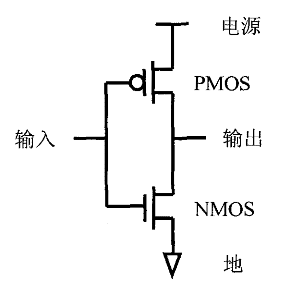
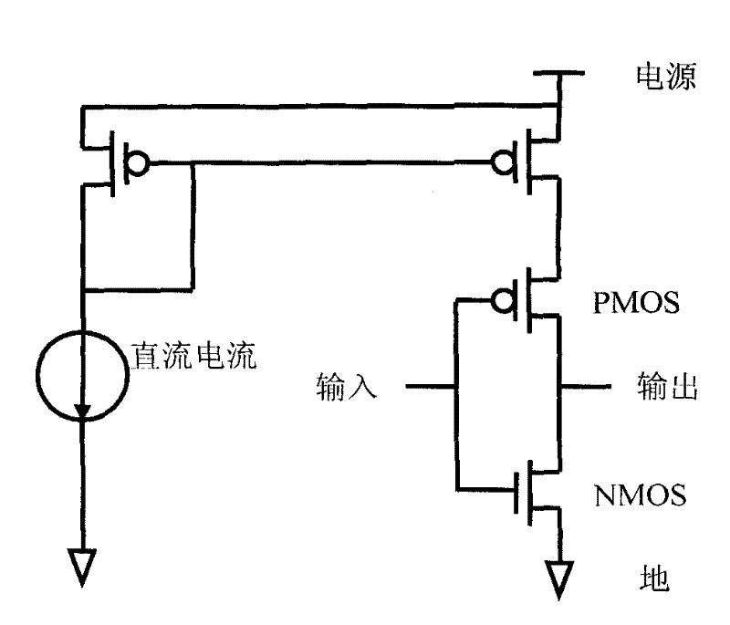
[0017] The specific implementation manner of the present invention will be further described below by taking a traditional CMOS gate circuit-inverter as an example in conjunction with the accompanying drawings.
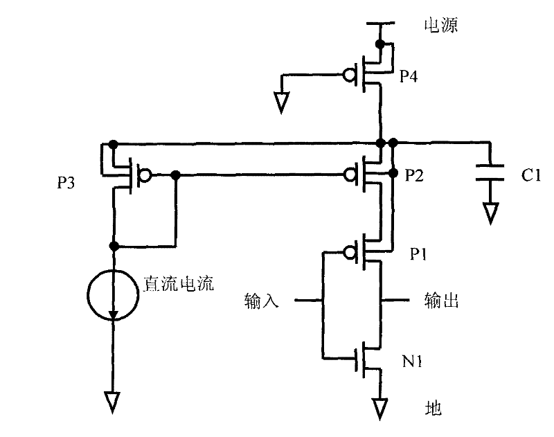
[0018] Please see image 3 A circuit for reducing CMOS transient power consumption of the present invention includes a CMOS inverter formed by connecting a PMOS transistor P1 and an NMOS transistor N1. The PMOS transistor used is provided with a source, a drain, a gate and a base drawn out from its substrate common well (N well). The gate of the PMOS transistor P1 is connected to the gate of the NMOS transistor N1 and is an input terminal; the drain of the PMOS transistor P1 is connected to the source of the NMOS transistor N1 and is an output terminal; the source of the PMOS transistor P1 is connected to a high level , that is, the power supply level is connected; the drain of the NMOS transistor N1 is grounded.
[0019] In order to limit the transient current of t...
PUM
 Abstract
Description
Claims
Application Information
 - R&D
- Intellectual Property
- Life Sciences
- Materials
- Tech Scout
- Unparalleled Data Quality
- Higher Quality Content
- 60% Fewer Hallucinations
Browse by: Latest US Patents, China's latest patents, Technical Efficacy Thesaurus, Application Domain, Technology Topic, Popular Technical Reports.
© 2025 PatSnap. All rights reserved.Legal|Privacy policy|Modern Slavery Act Transparency Statement|Sitemap|About US| Contact US: help@patsnap.com


