Integration-type passive element and manufacturing method thereof

A technology of passive components and manufacturing methods, applied in semiconductor/solid-state device manufacturing, electrical components, electrical solid-state devices, etc., can solve the problem that the Q value of the inductance structure cannot be further improved, and the application value of integrated passive components is limited.

Active Publication Date: 2010-09-15
ADVANCED SEMICON ENG INC
View PDF0 Cites 13 Cited by
  • Summary
  • Abstract
  • Description
  • Claims
  • Application Information

AI Technical Summary

Problems solved by technology

As a result, the Q value of the inductor structure cannot be further improved due to thickness issues,

Method used


Image

  • Integration-type passive element and manufacturing method thereof
  • Integration-type passive element and manufacturing method thereof
  • Integration-type passive element and manufacturing method thereof

Examples


Embodiment Construction

[0023] In order to make the above-mentioned purposes, features and advantages of the present invention more obvious and understandable, the preferred embodiments of the present invention will be specifically cited below, together with the accompanying drawings, for a detailed description as follows:

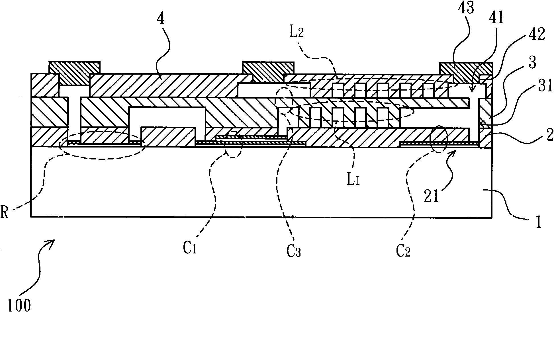
[0024] Please refer to figure 1 As shown, the integrated passive device (IPD) of the first embodiment of the present invention is similar to the existing thin film technology integrated passive device manufactured by physical phase deposition equipment in the semiconductor front-end wafer foundry industry, but the present invention changes to The semiconductor back-end packaging substrate equipment is used to manufacture integrated passive components, so that it has an inductive structure with a thickness greater than 5 microns, which is beneficial to reduce inductive loss and improve inductive efficiency, and can be applied to system-in-package (SIP) packaging. structure to impr...


PUM

PropertyMeasurementUnit
Thicknessaaaaaaaaaa
Thicknessaaaaaaaaaa
Thicknessaaaaaaaaaa

Abstract

The invention discloses an integration-type passive element and a manufacturing method thereof. The integration-type passive element is sequentially stacked with a first insulation layer, a second insulation layer and a third insulation layer on the upper surface of a substrate; a first circuit layer is arranged in the first insulation layer and comprises at least one capacitor structure and at least one resistor structure; a second circuit layer is arranged in the second insulation layer, has the thickness within 5 to 50 microns and forms at least one first inductor structure; and a third circuit layer is arranged in the third insulation layer, has the thickness within 5 to 25 microns and forms at least one second inductor structure. The integration-type passive element can be manufactured by adopting a semiconductor rear section encapsulation substrate device, has the capacitor structure with the thickness more than 5 microns, is further beneficial to reducing the inductor loss and improving the inductor efficiency and can improve the integration density of the passive element and reduce the element size.

Description

【Technical field】 [0001] The present invention relates to an integrated passive component and its manufacturing method, in particular to an integrated passive component with a thick inductor layer and its manufacturing method. 【Background technique】 [0002] Nowadays, in order to meet various high-density packaging requirements, the semiconductor packaging industry has gradually developed various types of packaging structures, among which various system in package (SIP) design concepts are often used to build high-density packaging structures. In the package structure of the system package type, two or more chips can be placed on the same package substrate to increase the chip assembly density. In addition, it is also possible to integrate several passive elements (passive elements) into a single integrated passive device (integrated passive device, IPD), so as to improve the utilization rate of the limited assembly area of ​​the substrate. [0003] According to different m...

Claims


Application Information

Patent Timeline
IPC IPC(8): H01L27/01H01L27/04H01L27/12H01L21/02
Inventor 苏清辉杨学安
Owner ADVANCED SEMICON ENG INC
Why Eureka
Try Eureka