
High density six transistor finfet SRAM cell layout

Inactive Publication Date: 2012-09-20
GLOBALFOUNDRIES INC
View PDF3 Cites 16 Cited by
  • Summary
  • Abstract
  • Description
  • Claims
  • Application Information

AI Technical Summary

Benefits of technology

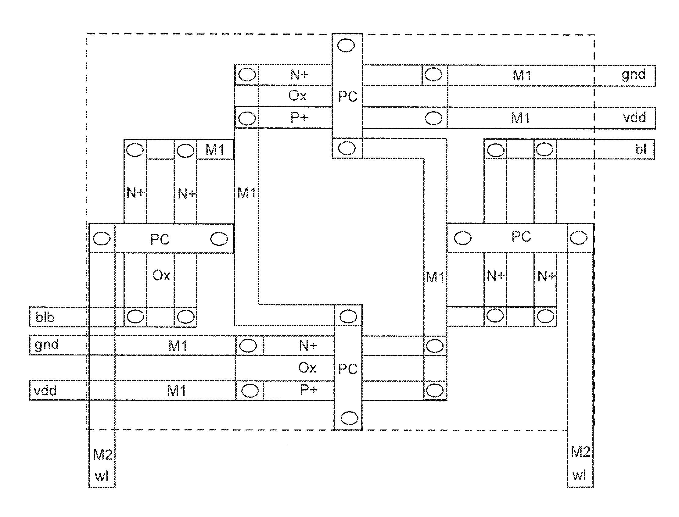
[0005]It is therefore an object of the present invention to provide an SRAM cell layout which can be scaled to a 15 nm or smaller minimum feature size to improve economy and performance but using conventional masks that do not limit reduction of bit-cell size or footprint and including FinFETs of improved robustness.
[0009]In summary, the invention comprehends an integrated circuit structure that may be manufactured simply at an arbitrarily small minimum feature size using currently available mask and implantation technology and that is usable as a logic element that may contain 2, 3 or 4 FinFET transistors comprising four conduction channel fins arranged in two pairs of fins, depending upon the impurity implantations made in each pair of fins, and which is particularly applicable to a six transistor SRAM bit-cell layout which is more compact than current designs and highly scalable while providing improved fidelity of fin formation. In such an application, it allows a more compact layout with more conveniently and reliably formed connections that can be scaled to an arbitrarily small footprint area at correspondingly increased integration density. The invention further comprehends the more compact SRAM bit-cell layout and the techniques of forming two pairs of differently oriented FinFET transistors and impurity implantations to form 2, 3 or 4 transistors from two pairs of fins or, preferably, six transistors from four pairs of fins such as for an SRAM bit-cell, and so on.

Problems solved by technology

For example, so-called hard drives are typically used for efficient long term storage of large amounts of data and programs but allow relatively rapid access thereto, usually in large blocks, even though such access generally requires a substantial number of clock cycles of the processor.
Such refresh operations may impose a longer (e.g. worst-case) access time.
Additionally, since SRAM response speed is critical, SRAMs are usually included in the integrated circuits which access them and can often occupy 50% or more of the chip area which, in turn, tends to limit the amount of other logic that can be provided unless bit-cell area / footprint is minimized.

Method used


Image

  • High density six transistor finfet SRAM cell layout
  • High density six transistor finfet SRAM cell layout
  • High density six transistor finfet SRAM cell layout

Examples


Embodiment Construction

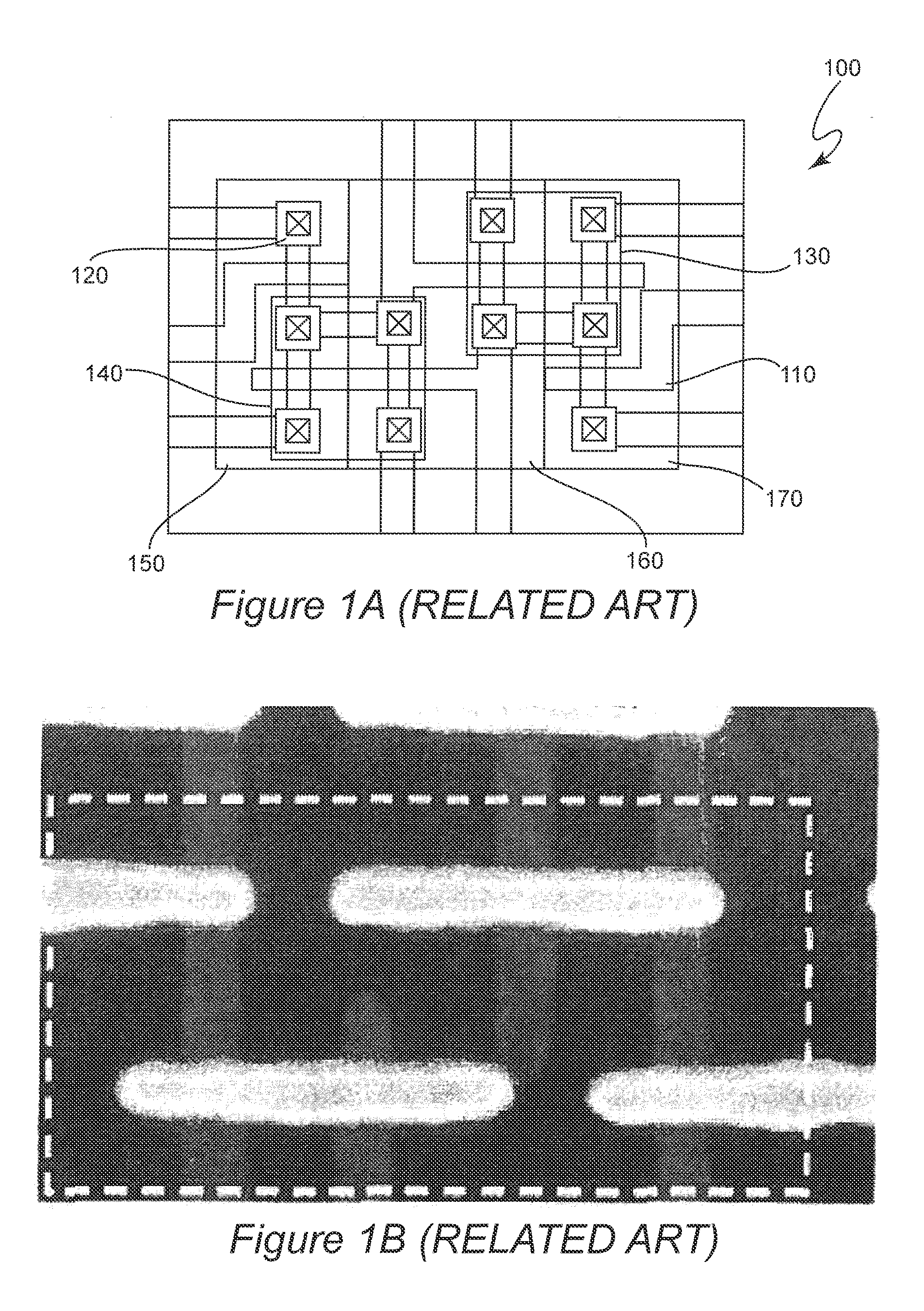
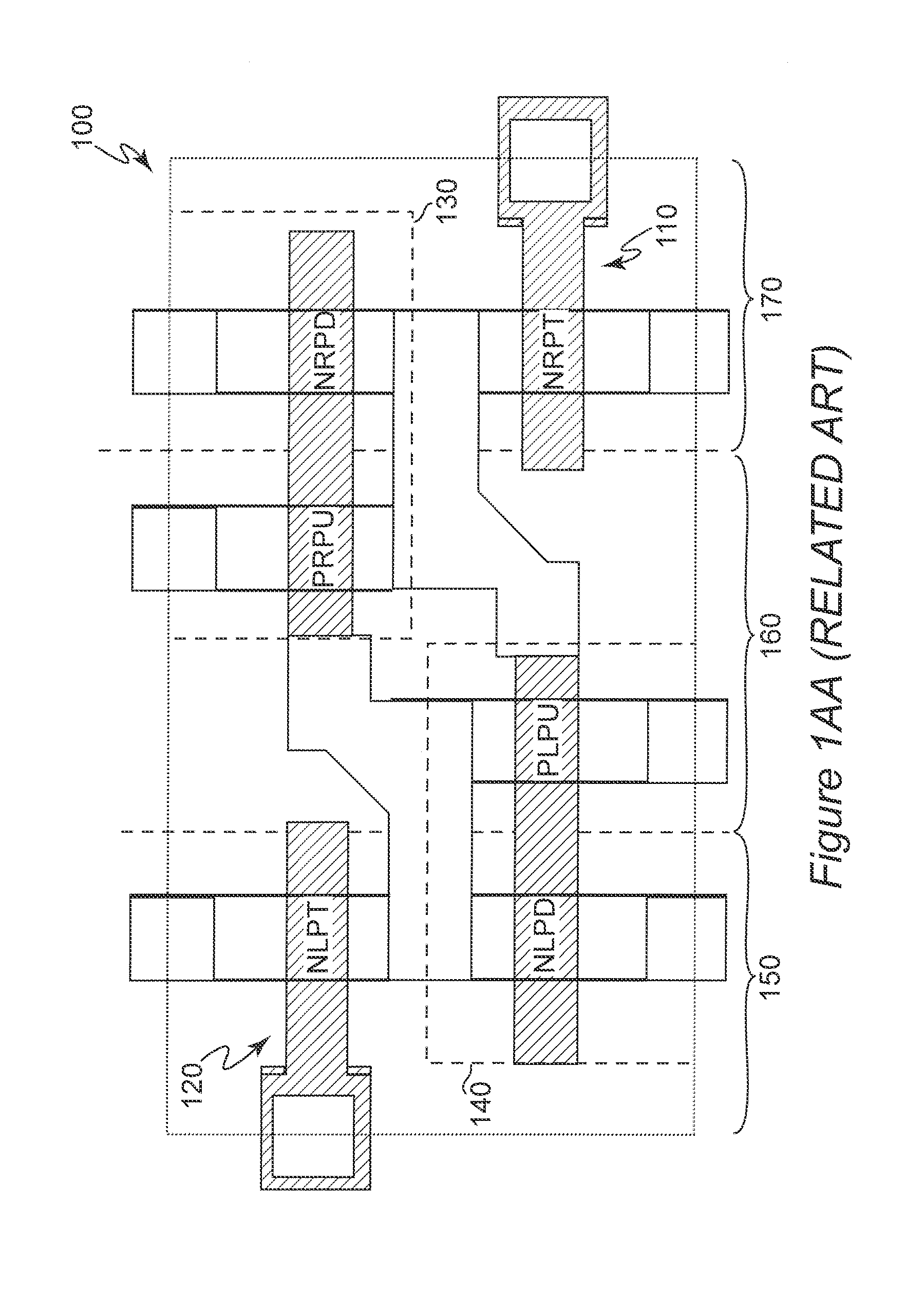
[0020]Referring now to the drawings, and more particularly to FIG. 1A, there is shown a plan view of the layout of a known SRAM cell including six transistors and sufficient to store a single bit (thus, sometimes referred to hereinafter as a bit-cell). FIG. 1AA is an enlarged schematic depiction of the plan view of the bit-cell layout of FIG. 1A. The transistors are indicated with the same reference numerals in both FIGS. 1A and 1AA. FIG. 1B is a scanning electron microscope (SEM) image of a device having the same layout but prior to the application of connections shown in FIG. 1A. The brighter, horizontal areas appearing in FIG. 1B are polysilicon gates while the darker, vertical areas of FIG. 1B are the FinFET fins.

[0021]As a compromise between performance and complexity, an SRAM memory cell usually comprises six transistors although as few as four transistors or eight or more transistors can be used in each SRAM cell. Using only four transistors requires inclusion of resistors wh...


PUM


Abstract

Dual orientation of finFET transistors in a static random access memory (SRAM) cell allows aggressive scaling to a minimum feature size of 15 nm and smaller using currently known masking techniques that provide good manufacturing yield. A preferred layout and embodiment features inverters formed from adjacent, parallel finFETs with a shared gate and different conductivity types developed through a double sidewall image transfer process while the preferred dimensions of the inverter finFETs and the pass transistors allow critical dimensions of all transistors to be sufficiently uniform despite the dual transistor orientation of the SRAM cell layout.

Description

FIELD OF THE INVENTION[0001]The present invention generally relates to integrated circuit logic structures and, more particularly, to static random access memory (SRAM) memory cells formed using FinFET transistors, requiring reduced chip area, and which can be fabricated at a minimum feature size of 15 nm or smaller using currently existing mask and impurity implantation technology.BACKGROUND OF THE INVENTION[0002]Digital memory devices are essential elements of any digital data processor. Modern digital data processors generally use at least several different types of memory devices which have been developed to answer different performance requirements within various functional portions of the data processing system. For example, so-called hard drives are typically used for efficient long term storage of large amounts of data and programs but allow relatively rapid access thereto, usually in large blocks, even though such access generally requires a substantial number of clock cycl...

Claims


Application Information

Patent Timeline
IPC IPC(8): H01L27/12H01L21/8234H01L27/11
CPCH01L21/845H01L27/1211H01L27/1104H10B10/12
Inventor DIXIT, ABHISEK
Owner GLOBALFOUNDRIES INC
Learn More