Design method of NES (Nintendo Entertainment System) emulator used on TV set top box

A design method and simulator technology, applied to color TV parts, TV system parts, TVs, etc., to achieve the effects of low hardware configuration requirements, high execution efficiency, and convenient transplantation

Inactive Publication Date: 2010-09-15
FUJIAN NEWLAND COMM SCI TECH
0 Cites 4 Cited by

AI-Extracted Technical Summary

Problems solved by technology

Due to the difference in hardware, NES games can only be used on dedicated NES hosts at present, and a game generally requires a cassette. ...

Abstract

The invention relates to a design method of an NES (Nintendo Entertainment System) emulator used on a TV set top box, which comprises the following steps of: 1. emulating commands of a 6502cpu (Central Processing Unit); 2. emulating a graphic processing unit (PPU), which is a core NES component; 3. optimizing a graphic buffering mechanism; 4. emulating a sound processor; 5. emulating a joystick controller; and 6. analyzing file formats of NES games. The invention realizes the support to the NES games through a common set top box, and ensures that set top boxes of different types can be directly upgraded into an NES game machine as long as using the NES emulator designed according to the design method, thereby effectively meeting the user's requirements for games of various types.

Application Domain

Technology Topic

Image

  • Design method of NES (Nintendo Entertainment System) emulator used on TV set top box

Examples

  • Experimental program(1)

Example Embodiment

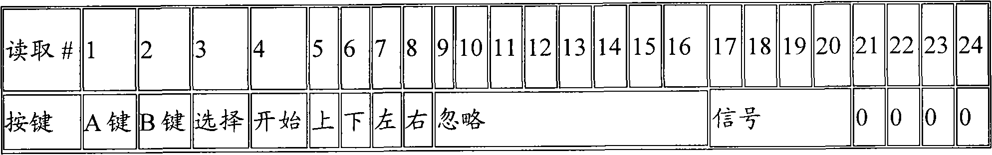
[0029] The design method of the NES emulator used on the TV set-top box of the present invention includes: 1. The simulation of 6502 cpu instructions; 2. The simulation of the PPU graphics processor, the core component of NES; 3. The optimization of the graphics buffer mechanism; 4. The simulation of the sound processor; 5. The simulation of the handle controller; and, the analysis of the NES game file format.
[0030] 1. Simulation of 6502cpu: This part uses pure C language to simulate 131 different instructions of 6502, and does not use assembly language related to the set-top box processing chip to describe it in order to further improve the portability of the entire simulator. Although the running speed of pure C language is slower than the 6502 simulator written in assembly language, it can be effectively and quickly transplanted to different STB platforms (different STB platforms have different CPU types and different instruction sets) . At the same time, in order to make up for the lack of speed and accelerate the speed of instruction simulation, a large number of inline functions and #define macro definitions are used, making its running speed basically reach about 80% of the efficiency of using assembly language.
[0031] The specific method includes the following steps:
[0032] Step 1: Obtain the operation code of 6502ROM:
[0033] The first thing to execute ROM is to get the opcode. Obtain the byte pointed to by the instruction pointer (IP) of the CPU. This byte is the opcode. Depending on the opcode, you may need to obtain operands or save this part for execution. For an 8-bit processor such as 6502CPU (8-bit processer), the code format for obtaining the opcode is as follows:
[0034] needOpcode=pProgramROMBank[wInstructionPointer];
[0035] The memory segment pointed to by pProgramROMBank is the ENS ROM that was read in at the beginning, and wInstructionPointer is the instruction pointer (where the instruction is currently executed). After the above execution, needOpcode will save this opcode in a numeric value.
[0036] Step 2: Decode and execute the opcode:
[0037] After obtaining the opcode byte, it needs to be decoded and executed. Since the system NES to be simulated is an 8-bit processor, the "word" in the opcode is just an instruction, and the decoding process only needs to be considered in terms of bytes (8-bit bit).
[0038] For example, for 6502Cpu, the value 29h is a table of AND instructions. In this way, it performs AND immediately, which means that it will perform an AND operation between the accumulator register and the immediate value after the opcode byte. Because of this 6502CPU simulator, it is necessary to perform an AND on the accumulator after the AND opcode byte. Then you need to increase the IP, plus or minus the number of clock cycles taken to execute that particular instruction.
[0039] The following is the code of the AND operation, the other operations are the same as its operation.
[0040] switch(needOpcode)
[0041] {
[0042] case 0x29:
[0043] byOperand1=pProgramROMBank[wInstructionPointer+1];
[0044] A&=byOperand1;
[0045] The above is a simulation of the AND instruction in 6502CPU
[0046] break;
[0047]. case xxxx:
[0048] In other branches, it is the processing program of other opcodes, which is the same as the above method, which is processed according to the execution command defined by the standard 6205 instruction set
[0049] break;
[0050].
[0051].
[0052] }
[0053] wInstructionPointer+=wNumBytesForOpcode;
[0054] The above line of program simulates the 6502 PC pointer.
[0055] dwCPUCycles-=dwNumCyclesForOpcode;
[0056] The above line of program simulates the clock cycle of the 6502 CPU.
[0057] In this way, the entire 6502CPU 131 instructions can be simulated.
[0058] Step 3: Execution interrupt:
[0059] When a specific instruction in the program is executed, a software interrupt occurs. The BRK instruction is used to execute interrupts in the 6502CPU of the NES emulator.
[0060] When an interrupt occurs, the NES emulator saves the instruction pointer and the flag register, and then finds a new value in a specific memory area and assigns it to the instruction pointer. Each terminal has its assigned address, so the NES emulator gets the value from that location and assigns it to the instruction pointer. Then the program continues execution from this point. The 6502CPU of the NES emulator has three interrupts. The new value of the instruction pointer depends on the memory address where the interrupt occurred.
[0061] FFFAh=NMI(VBlank)
[0062] FFFCh=RESET
[0063] FFFEh=IRQ/BRK(software)
[0064] Therefore, when the VBlakn occurs when the NES interrupt is simulated, the CPU will:
[0065] 1) Push the current value of the instruction pointer onto the stack.
[0066] 2) Push the current value of the flag register onto the stack.
[0067] 3) Get the value in the word FFFah and copy it to the instruction pointer.
[0068] The details are as follows:
[0069] ++PC;
[0070] PUSHW(PC);
[0071] SETF(FLAG_B);
[0072] PUSH(F);
[0073] SETF(FLAG_I);
[0074] Among them, PUSHW and PUSH are operations of pushing values ​​onto the stack, SETF is the register flag bit of the set CPU, and PC is the instruction counter of the CPU.
[0075] Step 4: Read and write memory:
[0076] There are two ways to read and write memory in the simulator. One is to get the opcode and the operand of the opcode (a simple way to read the memory, there is no simulation behavior in this process). Another method is to read and write memory when instructions are executed (this is the focus of emulator simulation). The instructions that can be read and written in the NES 6502 CPU are LDA (read) and STA (write). For these instructions in the simulation process, the main focus is on the read or write address and the specific occurrence time (read and write timing). A specific memory address (perhaps a register, memory mirror, or any other address owned by the system). The following example illustrates the method of reading a process from memory. Write memory and read memory in a similar way.
[0077] BYTE ReadMemory(WORD wAddress)
[0078] {
[0079] switch(wAddress)
[0080] {
[0081] case 0x2002:
[0082] The above is for the read operation of the PPU status register in the 6502CPU
[0083] break;
[0084] case 0x2004:
[0085] The above is for reading a byte of sprite memory in 6502CPU
[0086] break;
[0087] case xxxx:
[0088] The above is for other registers, memory mirroring, or any other system in 6502CPU
[0089] Read operation of owning address.
[0090] break;.
[0091] }
[0092] }
[0093] Step 5: Complete continuous reading of instructions:
[0094] This simulator specifies the operating efficiency and speed of the entire simulator by selecting the time and location to execute the cyclic task. After drawing a scan line, after drawing an entire screen, or even after any instruction, the more cyclic tasks, the more performance The more loss, but the higher the accuracy. If the cycle tasks are reduced, the speed of the simulator will increase but some accuracy will be lost. The clock cycle required by each scan line is expressed by the following function:
[0095] NumCyclesPerScanline=(CPUFrequency/RefreshRate)/
[0096] NumScanlinePerFrame
[0097] NumCyclesPerScanline
[0098] CPUFrequency is the frequency of the set-top box chip.
[0099] RefreshRate is the refresh rate of the simulator.
[0100] NumScanlinePerFrame is the number of scan lines in each frame of the simulator.
[0101] NumCyclesPerScanline is the clock cycle required for each scan line.
[0102] 2. Simulation of PPU graphics processor, including: simulation of PPU timing, including base frequency, CPU frequency, total scan line number, total scan line period, horizontal scan period, horizontal blank period, end period, frame period, Simulation of frame IRQ cycle, frame rate and frame time; simulation of the actual reading method of the stored pattern table; simulation of the reading method of the named table and named table image; simulation of the reading method of the attribute table; Palette, palette mirroring, background scrolling, screen and animation layered operation simulation; simulation of animation and animation RAM reading and operation; access to VRAM operation mode and access to PPU RAM when the screen is refreshed Simulation of operation mode.
[0103] 3. Optimize the graphics buffer mechanism. Because the image format of NES is special and cannot be used directly, an important part of the emulator is to convert the image data input during the running of the NES game into a common format. Shown on the screen of the set-top box. The principle of the graphics buffer mechanism is: when the PPU graphics processor refreshes the screen image, it does not read data from the NES video VROM every time, but writes the NES format image data into the NES video in the NES emulator. When the memory is in memory, the data is converted into a format that can be recognized by the set-top box at one time and stored in the buffer, so that when the screen image is refreshed, the image data that has been converted into a format that can be recognized by the set-top box can be directly read in the buffer, and the data is buffered The modification only occurs when the NES emulator modifies the video VROM. The frequency of this operation mode is far lower than the frequency of screen refresh, and the efficiency of the entire image drawing is greatly improved.
[0104] 4. Sound processor simulation: The integrated CPU of the NES emulator contains a 4-channel sound processor (2A03), which provides quasi-simulated sound for playing music. Including 4 channels: 2 square waves, one triangle wave and one noise generation channel. This simulator mainly extracts the square wave and triangle wave data among them. Through the principle of wave superposition, the waveform sample data of all channels , Mixed into a wave, and then played the corresponding audio data through the audio input driver of the set-top box.
[0105] The specific implementation steps in this process are:
[0106] Step 1. First, read the eigenvalues ​​of the square wave and triangle wave from the sound register, and then calculate the wavelength of the wave through the eigenvalues;
[0107] Step 2. Calculate the working cycle of the wave. This is how many times the wavelength should be repeated until the end of the wave. Similarly, this is also read from the sound register;
[0108] Step 3. Calculate the output volume, which is read from the sound register, which can be considered as the amplitude of the wave;
[0109] Step 4. Move forward along the wave and write the data to the Buffer. The ratio of samples determines the number of bytes written to the buffer. Write the same number of samples in the CPU frame to the buffer. In the next frame, continue writing Enter the remaining data until you finish writing all the calculated wave data.
[0110] 5. Simulation of handle controller: NES supports many kinds of input devices, mainly including handle, light gun, 4 adapters and joystick. The NES emulator is mainly aimed at the simulation of the joystick controller and the simulation of the joystick controller, mapping part of the key values ​​of the remote control of the set-top box to the buttons on the joystick controller of the NES emulator (respectively up, down, left and right) , A key, b key, start, select and other keys), the input remote control code value is converted into a format recognized by NES for processing through the emulator, the format is shown in the following table.
[0111]
[0112] 6. Analysis of NES game file format: In this regard, it is mainly composed of two ways. One is that the set-top box supports the file system, and the NES game file is read by the file system, and parsed according to the corresponding NES format. ; The second is to simulate the NES file as an array of data on the set-top box that does not support the file system, and parse it according to the corresponding NES format. The NES file is the image used to store the NES cassette in the simulation. Here is one. The structure of the NES file.
[0113] Offset
[0114] Offset
[0115]
[0116] Analyze according to the above format, you can get the NES data.

PUM

no PUM

Description & Claims & Application Information

We can also present the details of the Description, Claims and Application information to help users get a comprehensive understanding of the technical details of the patent, such as background art, summary of invention, brief description of drawings, description of embodiments, and other original content. On the other hand, users can also determine the specific scope of protection of the technology through the list of claims; as well as understand the changes in the life cycle of the technology with the presentation of the patent timeline. Login to view more.

Similar technology patents

Classification and recommendation of technical efficacy words

  • Easy to transplant
  • Improve execution efficiency

Computing group structure for superlong instruction word and instruction flow multidata stream fusion

InactiveCN101021778AAvoid wasting storage bandwidthImprove execution efficiencyConcurrent instruction executionArchitecture with multiple processing unitsData bufferInstruction sequence
Owner:NAT UNIV OF DEFENSE TECH
Why Eureka
Try Eureka