Method for manufacturing printed circuit board and printed circuit board

A technology of printed circuit board and manufacturing method, which is applied in the direction of multi-layer circuit manufacturing, printed circuit components, and the formation of electrical connection of printed components, etc.

Active Publication Date: 2012-05-23
HUAWEI TECH CO LTD
View PDF6 Cites 0 Cited by
  • Summary
  • Abstract
  • Description
  • Claims
  • Application Information

AI Technical Summary

Problems solved by technology

[0003] The inventor found in the process of implementing the present invention that: in order to solve the limitations of board thickness, through-hole plating ability and other issues on the production of multi-layer PCB, the prior art uses the The Plating Through Hole (PTH) of the sub-board is filled to prevent the conductive paste from flowing into the PTH hole and affect the hole diameter and hole depth. This implementation is mainly used for high-density surface mount devices such as modules and carrier boards. In the case of miniaturization, plug-in devices cannot be realized

Method used


Image

  • Method for manufacturing printed circuit board and printed circuit board
  • Method for manufacturing printed circuit board and printed circuit board
  • Method for manufacturing printed circuit board and printed circuit board

Examples


Embodiment Construction

[0030] The following will clearly and completely describe the technical solutions in the embodiments of the present invention with reference to the accompanying drawings in the embodiments of the present invention. Obviously, the described embodiments are only some, not all, embodiments of the present invention. Based on the embodiments of the present invention, all other embodiments obtained by persons of ordinary skill in the art without making creative efforts belong to the protection scope of the present invention.

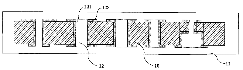
[0031] figure 1 A schematic structural diagram of a sub-board used in an embodiment of the present invention, such as figure 1 As shown, the metallized hole 12 is provided on the sub-board 11, and the hole wall 121 and the hole plate 122 of the metallized hole 12 are made of conductive materials to conduct electrical signals. The conductive material can specifically be a metal material with good electrical conductivity. The hole wall 121 is located in the h...


PUM


Abstract

The invention discloses a method for manufacturing a printed circuit board and the printed circuit board. The method comprises the following steps of: filling a resin material into a metallization hole of a first sub board and a metallization hole of a second sub board respectively to form depth controlled plug holes; filling conductive slurry at an opening of a bonding device sandwiched between the first sub board and the second sub board, wherein a hole disc of the metallization hole of the first sub board is electrically connected with a hole disc of the metallization hole of the second sub board through the conductive slurry; and pressing the first sub board, the bonding device and the second sub board to form the printed circuit board. According to the method, the depth controlled plug holes in the metallization holes of the first sub board and the second sub board block the conductive slurry from flowing into the metallization holes so that the depths and diameters of the metallization holes are protected and the metallization holes can realize plug of devices.

Description

technical field [0001] The embodiments of the present invention relate to the technical field of circuits, and in particular to a method for manufacturing a printed circuit board and the printed circuit board. Background technique [0002] As the functions of electronic products become more and more powerful, the large size, board thickness, and through-hole plating capabilities have reached the limit of equipment capabilities, making it difficult to improve the processing technology of multilayer printed circuit boards (PCB). The conventional processing technology of multi-layer PCB has brought great challenges. [0003] In the process of implementing the present invention, the inventor found that in order to solve the limitations of board thickness and through-hole plating ability on the production of multi-layer PCBs, the prior art fills the plating through holes (PTH) of the sub-board In fact, to prevent the conductive paste from flowing into the PTH hole to affect the ...

Claims


Application Information

Patent Timeline
Patent Type & Authority Patents(China)
IPC IPC(8): H05K3/46H05K3/42H05K1/11
Inventor 张顺李敬科常天海周水平
Owner HUAWEI TECH CO LTD
Why Eureka
Try Eureka