Packaging method for flip LED chips

A technology of LED chip and packaging method, which is applied in the direction of electrical components, circuits, semiconductor devices, etc., can solve the problems of waste, wire collapse, low coating efficiency, etc., achieve the improvement of color zone completion rate, improve product yield, coating The effect of uniform thickness

Active Publication Date: 2010-10-27
LEDMAN OPTOELECTRONICS
View PDF6 Cites 75 Cited by
  • Summary
  • Abstract
  • Description
  • Claims
  • Application Information

AI Technical Summary

Problems solved by technology

[0002] At present, there are mainly two conventional coating processes for phosphor powder on LED chips. The first process is to fill the bracket cup with LED chips fixed with phosphor, as shown in Figure 1. This process is mature, stable and easy to operate. , but the shape of the prepared phosphor is difficult to control, and the consistency is poor, resulting in obvious light spots and yellow halos on the product. When the light is split, the distribution of the color coordinate points between the products is relatively scattered, and there are many bins, which brings great harm to product storage and sales. It is a big difficulty, and the amount of phosphor used is large, and the waste ...

Method used


Image

  • Packaging method for flip LED chips
  • Packaging method for flip LED chips
  • Packaging method for flip LED chips

Examples


Embodiment Construction

[0023] In order to describe the technical content, structural features, achieved goals and effects of the present invention in detail, the following will be described in detail in conjunction with the embodiments and accompanying drawings.

[0024] Since the specific structure of the flip-chip LED chip is already in the prior art, the Chinese invention patent with the publication number CN100380694C and the invention name "A Flip-chip LED Packaging Method" has detailed introductions, so the specific embodiment of the present invention is only for flip-chip LED chips. The improved part of the LED chip packaging method is introduced.

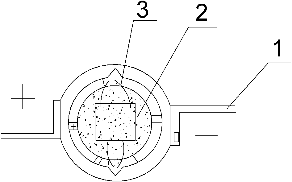
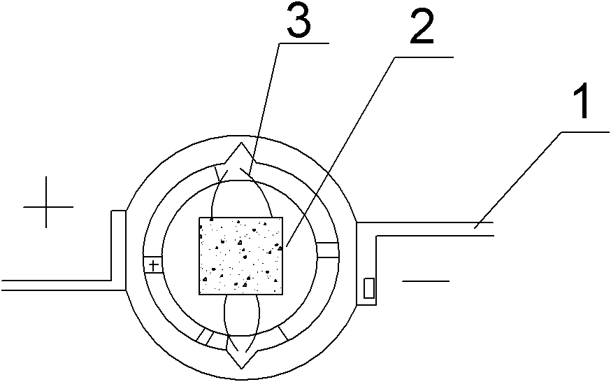
[0025] As an embodiment of the packaging method of the flip-chip LED chip of the present invention, please refer to FIG. 3, at least including the following steps:

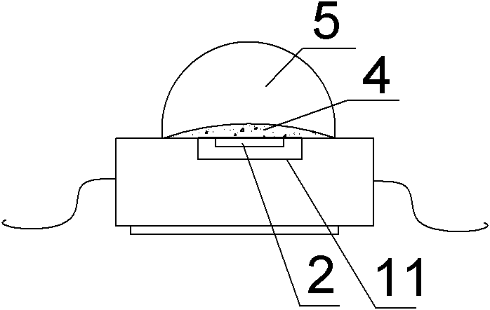
[0026] (a) coating the phosphor 4 on the surface of the light-emitting surface of the LED chip 2 by screen printing, and baking and curing the phosphor 4;

[0027] (b) Fixing the LED...


PUM


Abstract

The invention relates to a packaging method for flip LED chips, which belongs to the field of LED fabrication. The packaging method at least includes the following steps that: (a) phosphor is coated on the surface of an LED chip by screen printing, and is baked to become solidified; (b) the LED chip is fixed on a chip substrate, so that the electrodes of the LED chip are bonded with the electrodes of the chip substrate; (c) the LED chip and the chip substrate are fixed on a support and the bottom of a reflective cup; (d) wires are utilized to respectively connect the positive and the negative electrodes of the fixed chip substrate with the positive and the negative electrodes of the support; (e) a sealing mould or a lens covers on the support on which the LED chip and the chip substrate are fixed, and silica gel is filled; and (f) the whole structure is backed to become solidified. Since the used LED chip is a flip chip and the phosphor is coated on the surface of the LED chip before the wires are soldered, the product yield can be increased, and the screen printing technique can ensure that the thickness of the coated phosphor is more uniform, so the distribution of phosphor powder particles is more uniform.

Description

technical field [0001] The invention relates to a packaging method for flip-chip LED chips, which belongs to the field of LED manufacturing. Background technique [0002] At present, there are mainly two conventional coating processes for phosphor powder on LED chips. The first process is to fill the holder cup with LED chips fixed with phosphor, as shown in Figure 1. This process is mature, stable and easy to operate. , but the shape of the prepared phosphor is difficult to control, and the consistency is poor, resulting in obvious light spots and yellow halos on the product. When the light is split, the distribution of the color coordinate points between the products is scattered, and there are many bins, which brings great harm to the product storage and sales. It is a big difficulty, and the amount of phosphor used is large, and the waste is serious; the second process is to only coat the phosphor on the LED chip, as shown in Figure 2, the product produced by this proces...

Claims


Application Information

Patent Timeline
IPC IPC(8): H01L33/48H01L33/50H01L33/62
Inventor 李漫铁李志新扶韩伟
Owner LEDMAN OPTOELECTRONICS
Why Eureka
Try Eureka