Temperature-insensitive clock buffer and H-shaped clock tree circuit
What is AI technical title?
AI technical title is built by Patsnap AI team. It summarizes the technical point description of the patent document.
A clock buffer, sensitive technology, used in the field of circuits, can solve the problem of consumption, multi-routing resources, etc.
Active Publication Date: 2012-06-20
BEIJING PKUNITY MICROSYST TECH
View PDF0 Cites 0 Cited by
Summary
Abstract
Description
Claims
Application Information
AI Technical Summary
This helps you quickly interpret patents by identifying the three key elements:
Problems solved by technology
Method used
Benefits of technology
Problems solved by technology
However, for a design with useful clock skew (useful skew) technology applied, the delay of the clock signal from the clock source to the flip-flop is not required to be uniform, so the traditional clock network cannot solve the clock skew problem caused by temperature.
At the same time, the clock network design method needs to consume more precious routing resources
Method used
Image
Click on the blue label to locate the original text in one second.
Reading with bidirectional positioning of images and text.
Examples
Embodiment 1
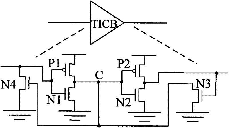
[0068] Embodiment 1. A temperature insensitive clock buffer (TICB), such as figure 1 shown, including:
[0069] The first and second inverters, the first NMOS transistor N4, and the second NMOS transistor N3;
[0070] The output end of the first inverter is connected to the input end of the second inverter; the input end of the first inverter is used as the input end of TICB, and the output end of the second inverter is used as the input end of TICB output terminal;
[0071] The drain of the first NMOS transistor N4 is connected to the input terminal of the first inverter, the gate is connected to the output terminal of the first inverter, and the source is connected to a low level;
[0072] The drain of the second NMOS transistor N3 is connected to the input terminal of the second inverter, the gate is connected to the output terminal of the second inverter, and the source is connected to a low level.
[0073] In this embodiment, the first inverter specifically includes: ...
Embodiment 2
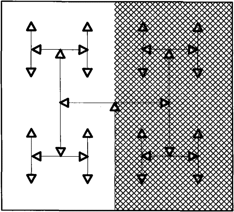
[0096] Embodiment 2, an H-shaped clock tree circuit, comprising:
[0097] Multiple TICBs in Embodiment 1; one of the TICBs is used as the root node of the H-shaped clock tree circuit, and the input end of the TICB is used as the input end of the H-shaped clock tree circuit. Starting from the TICB, each TICB The output end is connected to the input ends of the other two TICBs to form an H tree circuit.
[0098] That is, the TICBs at all levels in the clock tree are connected back and forth, and each level of TICBs drives the loads of two TICBs at the next level to achieve a balanced clock structure.
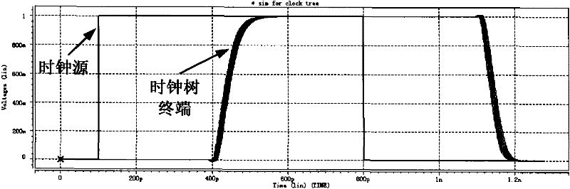
[0099] Due to the special structure of the TICB in the first embodiment, its delay hardly changes with temperature, so the clock skew caused by uneven temperature distribution inside the chip can be reduced.
[0100]In order to realize that the signal transmission delay on the clock tree is independent of temperature: when designing the TICB buffer, considering that the typical f...
PUM
Abstract
The invention provides a temperature-insensitive clock buffer (TICB) and an H-shaped clock tree circuit. The TICB comprises a first phase inverter, a second phase inverter, a first NMOS tube and a second NMOS tube, wherein the output end of the first phase inverter is connected with the input end of the second phase inverter; the input end of the first phase inverter is used as the input end of the TICB, and the output end of the second phase inverter is used as the output end of the TICB; the drain of the first NMOS tube is connected with the input end of the first phase inverter, the grid of the first NMOS tube is connected with the output end of the first phase inverter, and the source of the first NMOS tube is connected with a low level; and the drain of the second NMOS tube is connected with the input end of the second phase inverter, the grid of the second NMOS tube is connected with the output end of the second phase inverter, and the source of the second NMOS tube is connectedwith the low level. The H-shaped clock tree circuit comprises a plurality of TICBs. The technical scheme of the invention can resist temperature deviation and reduce clock skew caused by non-uniform temperature distribution, thereby ensuring the performance of an integrated circuit.
Description
technical field [0001] The invention relates to the field of circuits, in particular to a temperature-insensitive clock buffer and an H-type clock tree circuit. Background technique [0002] According to ITRS2009 data, the power consumption density of high-performance processors has reached 120W / cm 2 , such a high power density causes the chip temperature to be too high. At the same time, the use of a large number of on-chip memories, multiple power domains, dynamic voltage frequency scaling (DVFS), clock gating and other technologies make the temperature distribution in the chip very uneven. In some processors, the temperature difference can even reach 77 degrees Celsius. [0003] Since resistances of CMOS (Complementary Metal Oxide Semiconductor, Complementary Metal Oxide Semiconductor) transistors and metal interconnection wires are sensitive to temperature, changes in temperature will affect circuit delays. The uneven temperature distribution in the chip will cause th...
Claims
Application Information
Patent Timeline
Application Date:The date an application was filed.
Publication Date:The date a patent or application was officially published.
First Publication Date:The earliest publication date of a patent with the same application number.
Issue Date:Publication date of the patent grant document.
PCT Entry Date:The Entry date of PCT National Phase.
Estimated Expiry Date:The statutory expiry date of a patent right according to the Patent Law, and it is the longest term of protection that the patent right can achieve without the termination of the patent right due to other reasons(Term extension factor has been taken into account ).
Invalid Date:Actual expiry date is based on effective date or publication date of legal transaction data of invalid patent.

