
Substrate for an LED submount, and LED submount

A technology for light-emitting diodes and diode elements, which is applied to the substrate for light-emitting diode bases and the field of light-emitting diode bases, and can solve problems such as difficult terminal separation.

Active Publication Date: 2012-06-13
OSRAM GMBH
View PDF0 Cites 0 Cited by
  • Summary
  • Abstract
  • Description
  • Claims
  • Application Information

AI Technical Summary

Problems solved by technology

However, in the case of a small number of LED mounting positions and LEDs applied thereto (for example more than four LEDs), it becomes difficult to separate the terminals while compatible with a compact design.

Method used


Image

  • Substrate for an LED submount, and LED submount
  • Substrate for an LED submount, and LED submount
  • Substrate for an LED submount, and LED submount

Examples


Embodiment Construction

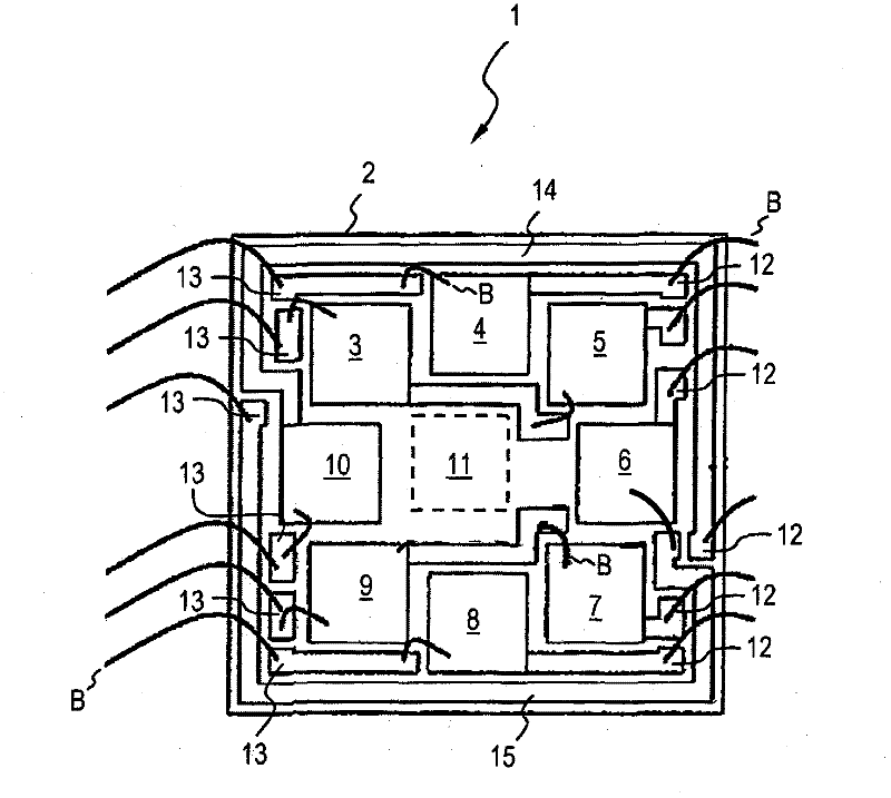
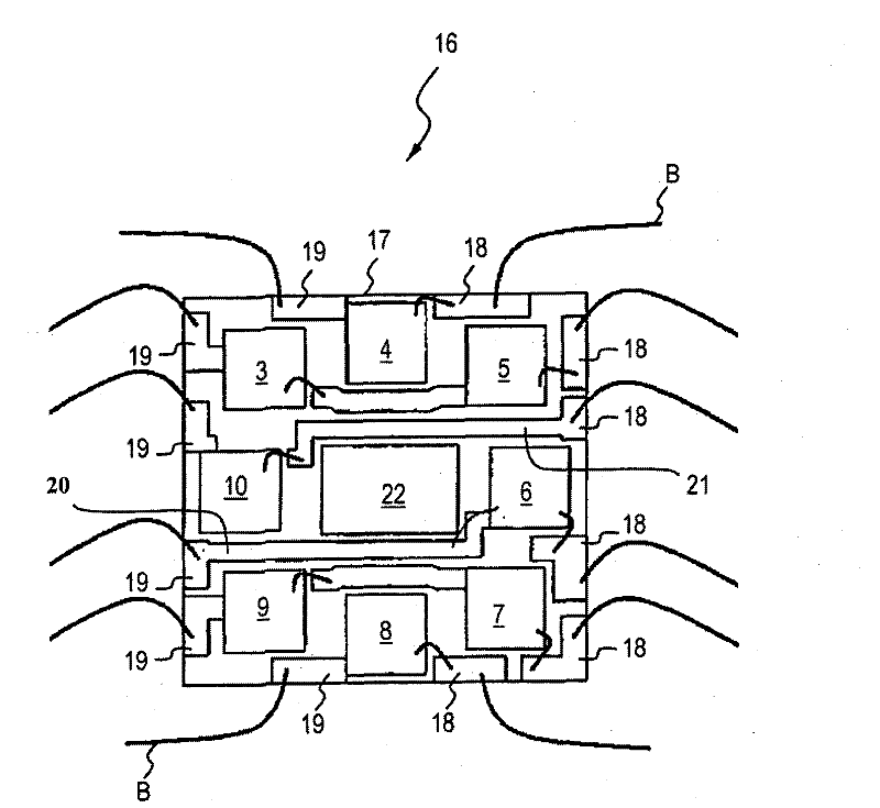
[0038] figure 1 An LED mount 1 is shown, in which eight LEDs or LED chips 3 - 10 are applied on a substrate 2 at corresponding LED mounting locations (not shown). Specifically, it is a white LED 3 , a green LED 4 , a white LED 5 , a yellow LED 6 , a white LED 7 , a blue LED 8 , a white LED 9 and a red LED 10 . White LEDs 3 , 5 , 7 , 9 and single-color LEDs 4 , 6 , 8 , 10 are arranged alternately in a ring on the outside and viewed in the circumferential direction. This results in a compact arrangement of the LED chips 3 - 10 on the substrate 2 , which facilitates good color mixing. Mounting locations 11 remain on the inside for non-LED components, such as color sensors, brightness sensors, temperature sensors or encoders (not shown) for active chromaticity coordinate adjustment.

[0039] The arrangement of the LEDs 3-10 (and thus the arrangement of the LED mounting locations) can also be described by means of a (3×3) matrix pattern, where the LEDs 3-10 are arranged on the ou...


PUM


Abstract

The invention relates to a substrate for an LED submount, having a plurality of mounting slots on the substrate surface thereof, and a plurality of pairs, each consisting of an electric anode connection and an electric cathode connection, wherein the anode connections are disposed on a first side section of the substrate surface, and the cathode connections are disposed on a second side section of the substrate surface, comprising at least one connection distribution conductor, leading from a mounting slot to an electric connection past at least two further mounting slots.

Description

technical field [0001] The invention relates to a substrate for a light emitting diode base, a light emitting diode base and a light emitting diode light source with the light emitting diode base. Background technique [0002] When designing a light-emitting diode (LED) mount, ie the substrate on which at least one LED or LED chip is applied, it is often desirable for easier connection of the LED mount to separate the anode-side connections from the cathode-side connections. This applies especially if several bases are to be connected in series. However, in the case of a small number of LED mounting locations and LEDs applied thereto (for example more than four LEDs), it becomes difficult to separate the terminals while compatible with a compact design. Contents of the invention [0003] The object of the present invention is to provide a possibility that can be implemented in a simple manner to spatially separate the anode and cathode connections of the submount while ma...

Claims


Application Information

Patent Timeline
IPC IPC(8): H01L25/075H01L33/00F21K7/00F21K99/00H01L33/62
CPCH01L33/62H01L2224/48091H01L25/0753H01L2924/00014H01L2924/00
Inventor 扬·马费尔德斯特芬·施特劳斯
Owner OSRAM GMBH
Learn More