

Method for controlling processing process of STI (Shallow Trench Isolation) channel of wafer
A technology for shallow trench isolation and wafers, which is applied in semiconductor/solid-state device manufacturing, electrical components, circuits, etc., and can solve problems that affect product quality stability, increase production costs, and reduce yields
- Summary
- Abstract
- Description
- Claims
- Application Information
AI Technical Summary
Problems solved by technology
Method used
Image

Examples
Embodiment Construction
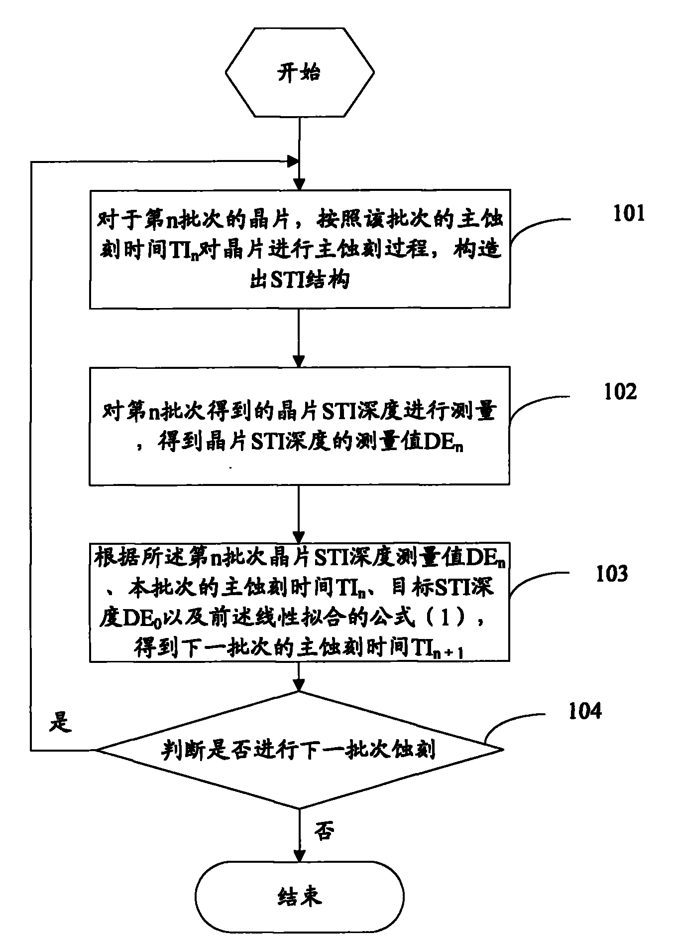
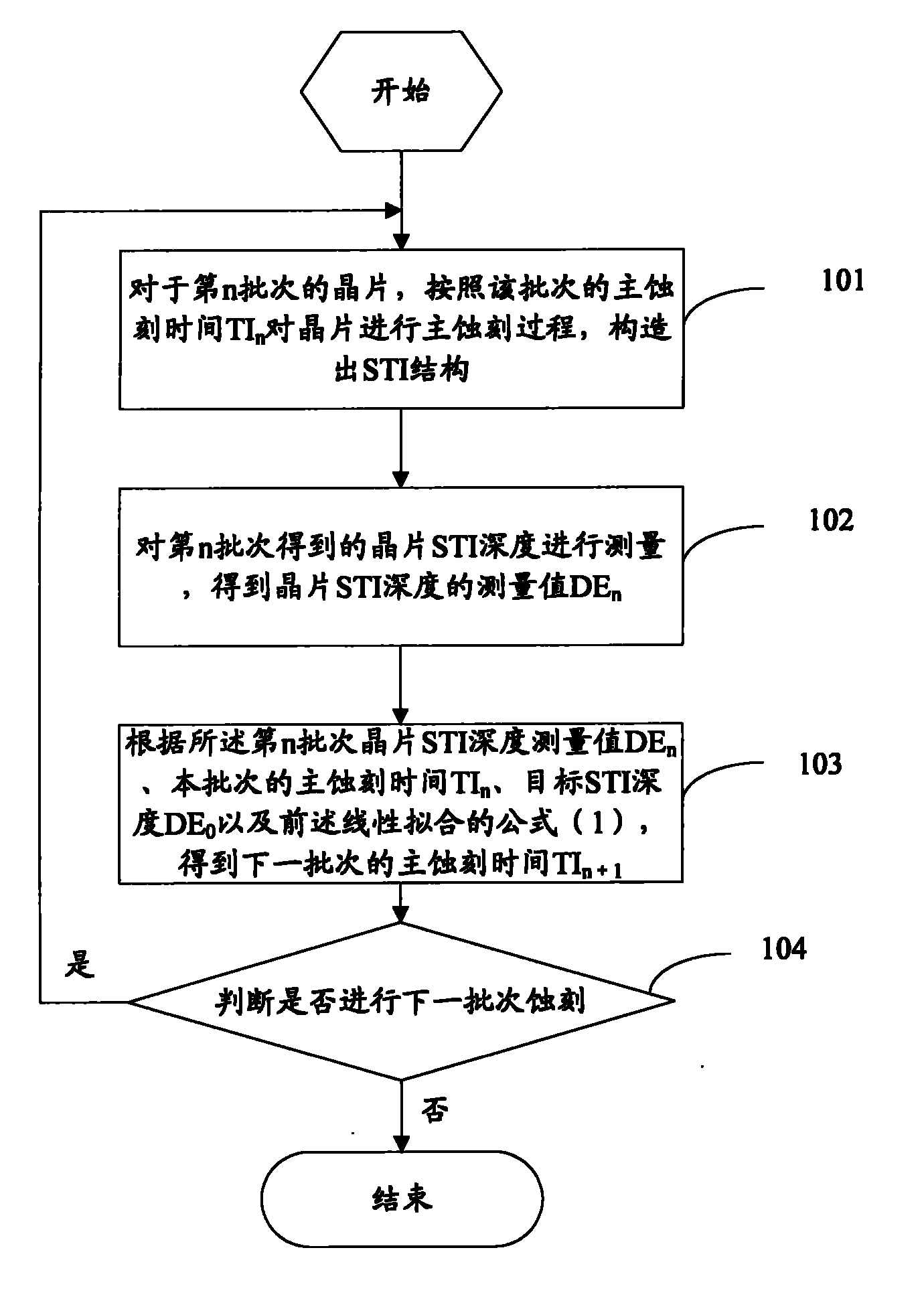
[0009] The inventor found through repeated research and experiments that under the same conditions, the depth of the STI is proportional to the time of the etching process (called the main etching process) used to generate the STI structure. Therefore, the inventor proposes a method of adjusting the etching time through a feedback mechanism, so as to achieve the purpose of controlling the depth of the STI.
[0010] In order to make the purpose, technical solution and advantages of the present invention clearer, the present invention will be further elaborated below in conjunction with the accompanying drawings.
[0011] The embodiment of the present invention studies the relationship between the STI depth and the time of the main etching process under the same conditions. The x-axis represents the time of the main etching process in seconds, and the y-axis represents the STI depth in nanometers (nm). Formula (1) can be obtained by linear fitting:
[0012] y=42.07x+1844.8, (1...
PUM
 Abstract
Description
Claims
Application Information