
Charge pump, charge pump booster circuit and operating method thereof

A boost circuit and charge pump technology, which is applied in the field of charge pump boost and charge pump, can solve the problem of insufficient charging and discharging of the charge pump, reducing the load capacity of the boost circuit of the charge pump, and the difference between the high and low voltage output of the charge pump. Small and other problems, to avoid the large drop in the difference between high and low voltage, increase the maximum operating frequency, and improve the effect of load capacity

Inactive Publication Date: 2012-12-12
HANGZHOU SILAN MICROELECTRONICS
View PDF0 Cites 0 Cited by
  • Summary
  • Abstract
  • Description
  • Claims
  • Application Information

AI Technical Summary

Problems solved by technology

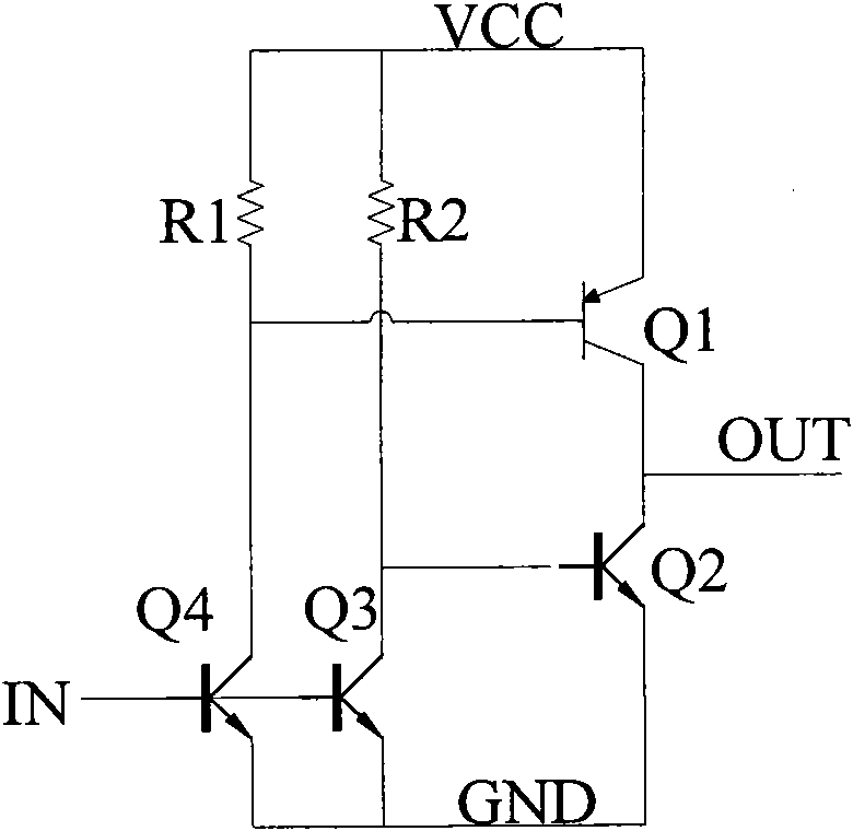
However, the high-frequency characteristics of ordinary PNP tubes are far worse than those of NPN tubes, so the maximum operating frequency of the charge pump booster circuit is limited by the PNP tube, and PNP tube Q1 cannot be turned off, or NPN tube Q2 is turned on for a long time, and PNP tube When the tube Q1 is turned off, the effective discharge time of the charge pump to the capacitor is shortened, the charging and discharging of the charge pump to the capacitor is insufficient, and the difference between the high and low voltage output of the charge pump becomes smaller, thereby reducing the load capacity of the boost circuit of the charge pump

Method used


Image

  • Charge pump, charge pump booster circuit and operating method thereof
  • Charge pump, charge pump booster circuit and operating method thereof
  • Charge pump, charge pump booster circuit and operating method thereof

Examples


Embodiment Construction

[0047] The content of the present invention will be further described below in conjunction with the accompanying drawings.

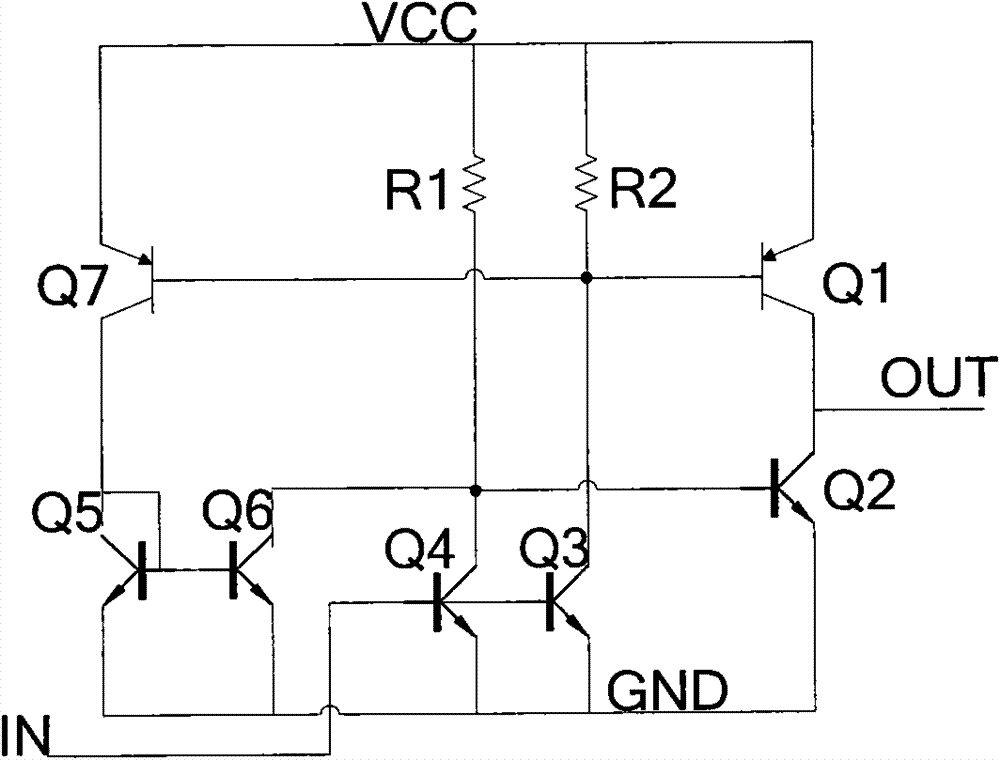
[0048] charge pump, such as Image 6 As shown, it includes: power supply VCC, first PNP transistor Q1, second PNP transistor Q3, NPN transistor Q2, the emitter of the first PNP transistor Q1 is connected to the power supply VCC, the base of the first PNP transistor Q1 is connected to the first potential Vb1, The base of the second PNP transistor Q3 is connected to the second potential Vb2, the base of the NPN transistor Q2 is connected to the clock signal CLK, the collector of the second PNP transistor Q3 and the emitter of the NPN transistor Q2 are grounded, and the collector of the first PNP transistor Q1 , The emitter of the second PNP transistor Q3 and the collector of the NPN transistor Q2 are connected as the output terminal OUT of the charge pump.

[0049] Further, the saturation current of the first PNP transistor Q1 is I 0 , the saturation cur...


PUM


Abstract

The invention provides a charge pump comprising a power supply VCC, a first PNP pipe Q1, a second PNP pipe Q3 and an NPN pipe Q2, wherein the emitting electrode of the first PNP pipe Q1 is connected with the power supply VCC; the base electrode of the first PNP pipe Q1 is connected with a first electric potential Vb1; the base electrode of the second PNP pipe Q3 is connected with a second electric potential Vb2; the base electrode of the NPN pipe Q2 is connected with a clock signal CLK; the collector electrode of the second PNP pipe Q3 and the emitting electrode of the NPN pipe Q2 are grounded; and the collector electrode of the first PNP pipe Q1, the emitting electrode of the second PNP pipe Q3 and the collector electrode of the NPN pipe Q2 are connected to be as the output end OUT of the charge pump. The invention simultaneously provides a charge pump booster circuit realized by utilizing the charge pump and an operating method thereof. Because the charging and discharging speed of the charge pump booster circuit does not depend on the PNP pipe but the switching speed of the NPN pipe in the charge pump, the switching speed of the charge pump is avoided being limited by the PNP pipe, the maximum operating frequency of the charge pump is increased, and the loading capacity of the charge pump booster circuit is improved.

Description

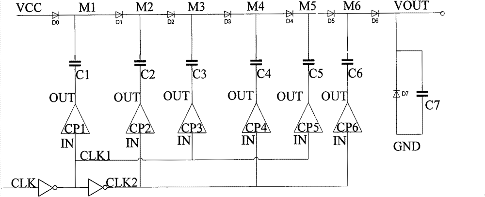
technical field [0001] The invention relates to power switch technology, in particular to charge pump and charge pump boosting technology. Background technique [0002] Commonly used charge pump boost circuits, such as figure 1 shown, including: [0003] a series of series diodes connected between the power supply and the output of the power supply; [0004] A series of charge pumps and capacitors, the input ends of the charge pumps are connected to the first clock signal, the output ends of each charge pump are connected to one end of their respective capacitors, and the other ends of the capacitors are connected to odd nodes of series diodes; [0005] A series of charge pumps and capacitors, the input ends of the charge pumps are connected to the second clock signal, the output ends of each charge pump are connected to one end of their respective capacitors, and the other ends of the capacitors are connected to the even-numbered nodes of the series diodes; [0006] The ...

Claims


Application Information

Patent Timeline
Patent Type & Authority Patents(China)
IPC IPC(8): H02M3/07
Inventor 郑烷胡铁刚
Owner HANGZHOU SILAN MICROELECTRONICS
Learn More