Array-type processor having delay adjusting circuit for adjusting a clock cycle in accordance with a critical path delay of the data path

a delay adjustment circuit and clock cycle technology, applied in the field of array-type processors, can solve the problems of limited processing capability, inability to improve processing capability, and difficulty in executing data processing at high speed, so as to improve operation efficiency and adjust cycle time. , the effect of improving the efficiency

Active Publication Date: 2013-03-19
RENESAS ELECTRONICS CORP
View PDF24 Cites 1 Cited by
  • Summary
  • Abstract
  • Description
  • Claims
  • Application Information

AI Technical Summary

Benefits of technology

[0066]In accordance with the present invention, cycle time of each configuration can be adjusted to a predetermined programmed value by the provision of a delay adjusting circuit. In accordance with the present invention, if preceding or succeeding cycle time can be shortened, then cycle time of a configuration having a large critical path delay can be elongated correspondingly, maximum operating frequency can be raised and processing efficiency can be improved.

Problems solved by technology

This microprocessor is such that since the number of instructions that can be executed simultaneously by a single processor is several at most, the degree to which processing capability can be improved is limited.
This means that processing capability cannot be improved.
In other words, with a data processing system in which application programs are switched among freely, various types of data processing can be executed but it is difficult to execute data processing at high speed because it is necessary to execute processing sequentially.
However, the total delay time is 1T and the critical path delay also is 1T.
This time is wasted time if processing efficiency is considered.
However, in a case where the critical path delay of every data path is different, it is necessary to make operating frequency conform to the maximum delay; operation at high speed in excess of this value of frequency is not possible.
In particular, if the variation in critical path delay is large, an arrangement having a small critical path will not execute any processing for a large part of cycle time.
In actuality, however, such allocation is technically difficult at present.
In general, therefore, it is difficult to adjust the cycle time of parallel processing processors and to improve operation efficiency.
In addition, for the reasons set forth above, with the related art it is difficult to implement adjustment of cycle time that takes the operation time of processor elements into account.
The problem is that a clock having a high speed in comparison with cycle time is required.

Method used


Image

  • Array-type processor having delay adjusting circuit for adjusting a clock cycle in accordance with a critical path delay of the data path
  • Array-type processor having delay adjusting circuit for adjusting a clock cycle in accordance with a critical path delay of the data path
  • Array-type processor having delay adjusting circuit for adjusting a clock cycle in accordance with a critical path delay of the data path

Examples


first example

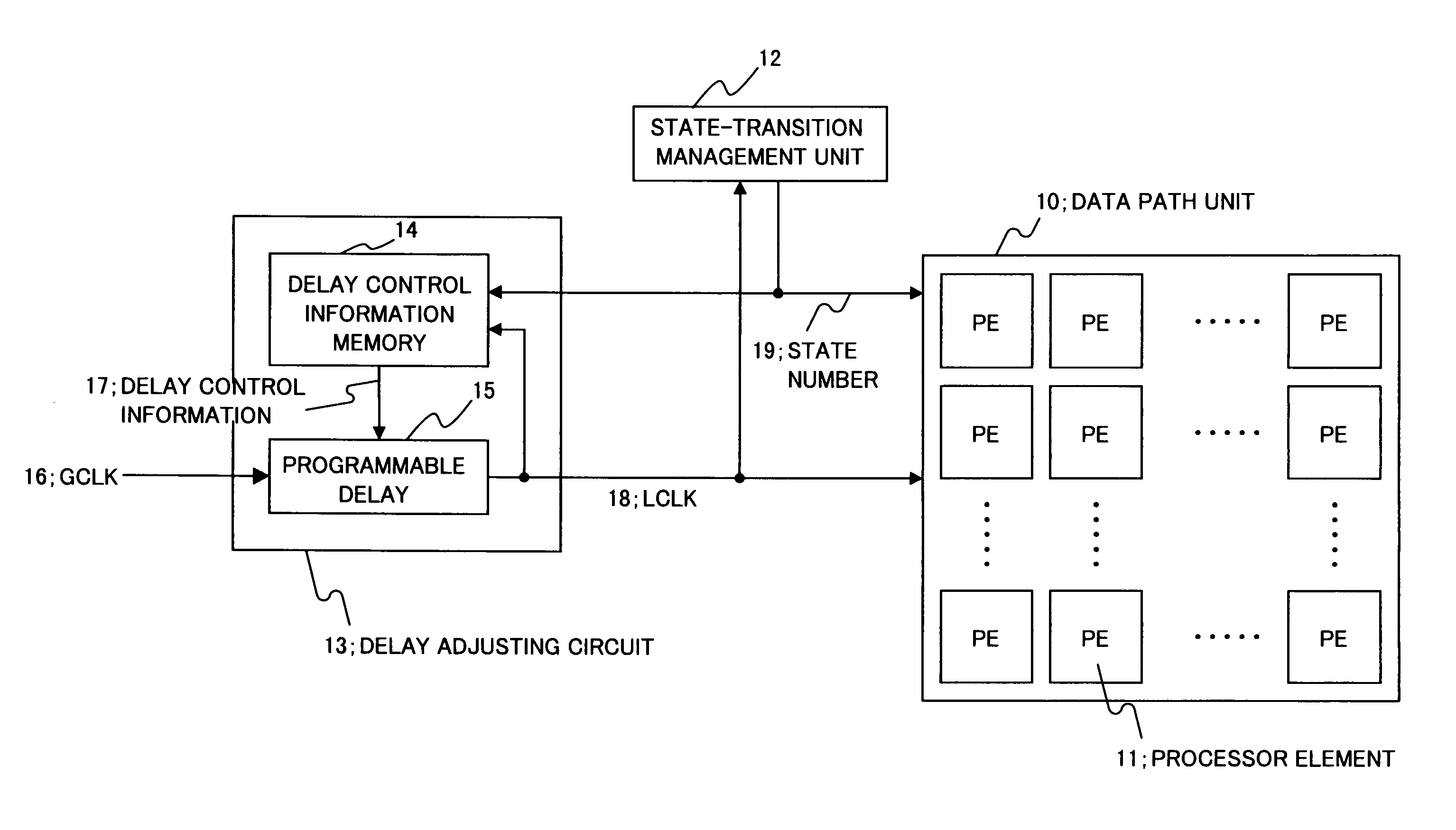
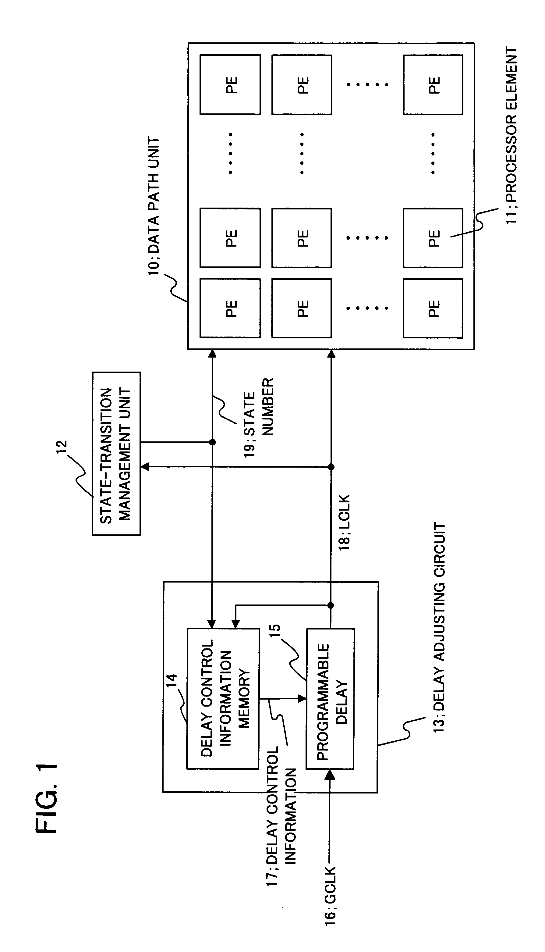
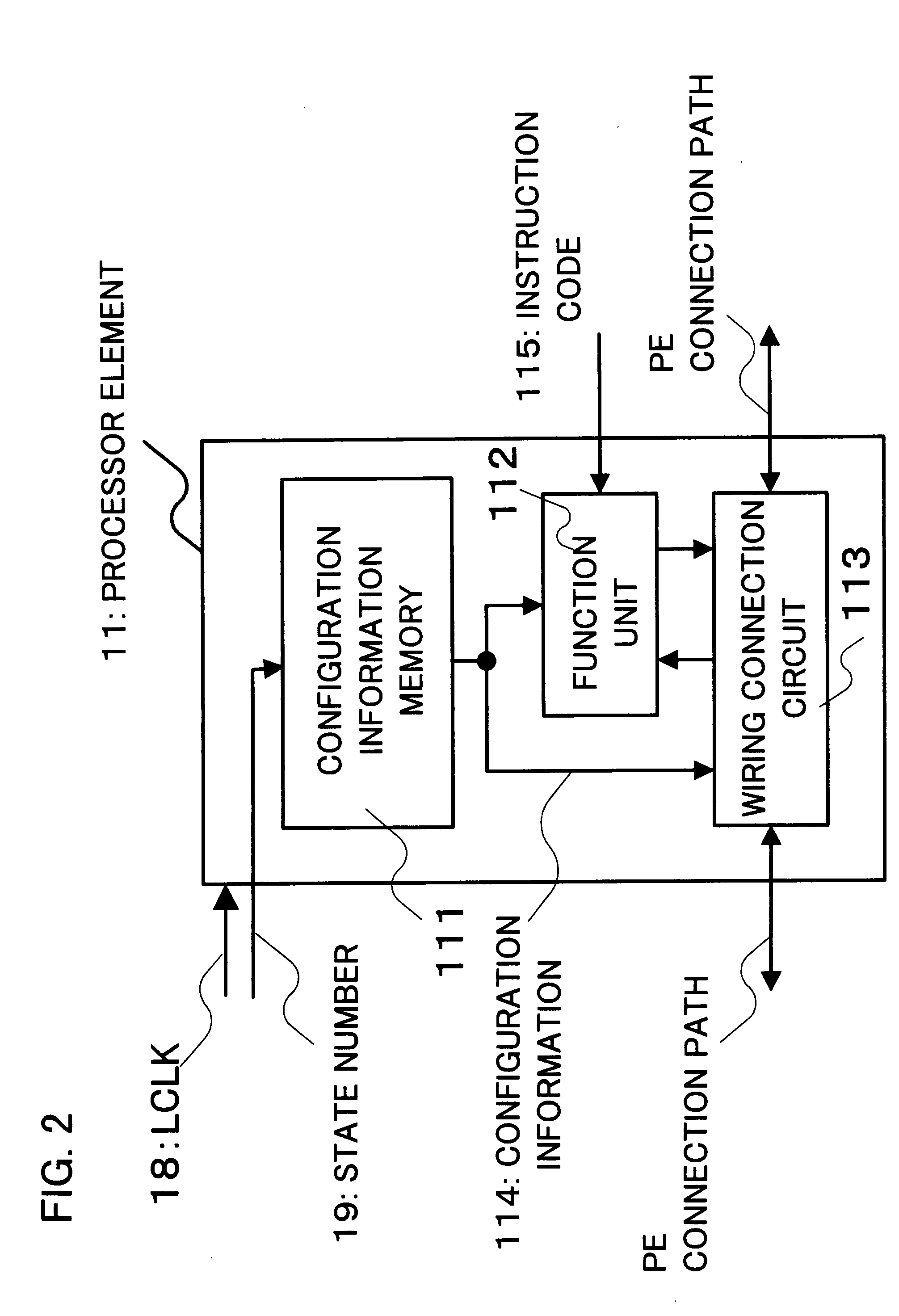
[0083]A first example of the present invention will now be described. FIG. 1 is a diagram illustrating the configuration of an array-type processor according to the first example of the present invention, and FIG. 2 is a diagram illustrating the configuration of a processor element (PE) in FIG. 1. The present invention will be described with reference to FIGS. 1 and 2.

[0084]As shown in FIG. 1, the array-type processor includes a data path unit 10, a state-transition management unit 12 and a delay adjusting circuit 13. The structures of the data path unit 10 and state-transition management unit 12 are similar to those shown in FIGS. 10 and 11 illustrating the array-type processor of the related art.

[0085]The state-transition management unit 12 includes a sequential unit and a state-transition table memory (neither of which are shown). The sequential unit of the state-transition management unit 12 reads a state number 19 out of the state-transition table memory and outputs the state n...

second example

[0134]A second example of the present invention will be described next. FIG. 4 is a block diagram in the second example of an array-type processor having the delay adjusting circuit of the present invention. The second example is obtained by providing the first example with a write control signal 20 and clock changeover signal 21.

[0135]The write control signal 20 and clock changeover signal 21 are input from outside the array-type processor of the invention and are utilized in order to control write (read-in) of a state number, configuration information, instruction code and delay control information (referred to below as “items of data” in this example) from outside the array-type processor of this invention and in order to control the synchronization timing of input / output signals to and from the exterior of the array-type processor.

[0136]The write control signal 20 is input to the delay control information memory 14 of the delay adjusting circuit 13, a state control information m...

third example

[0146]A third example of the present invention will be described next. FIG. 6 is a diagram illustrating the configuration of the third example. The third example is obtained by providing the first example with a data input / output control signal 22. The data input / output control signal 22 controls whether or not to perform a transfer between the data path unit 10 and registers or memories in an external circuit 23.

[0147]The delay control information memory 14 has data input / output control information in addition to delay control information. Further, the data input / output control information also is associated with the state number 19. In addition to the configuration information conforming to the state number 19, the delay adjusting circuit 13 outputs the data input / output control information from the delay control information memory 14 as the data input / output control signal 22.

[0148]FIG. 7 is a timing chart useful in describing the operation of the third example of the present inv...


PUM


Abstract

Disclosed is an array-type processor including a data path unit in which a plurality of processor elements are arranged in an array; a state-transition management unit that stores information for controlling changeover of data paths; and a delay adjusting circuit that adjusts delay of the input clock signal based upon information output from the state-transition management unit, and provides the delay-adjusted clock signal to the data path unit. The delay adjusting circuit has a delay control information memory and a programmable delay. The delay control information memory stores a plurality of items of delay control information, delay control information is read out using a configuration number supplied from the state-transition management unit as an address, and the delay control information is applied to the programmable array. The programmable delay delays the input clock signal by a delay time specified by the delay control information and provides the delayed clock signal to the data path unit.

Description

REFERENCE TO RELATED APPLICATION[0001]The present application is claiming the priority of the earlier Japanese patent application No. 2007-039624 filed on Feb. 20, 2007, the entire disclosure thereof being incorporated herein by reference thereto.FIELD OF THE INVENTION[0002]This invention relates to a processor that is capable of executing desired processing by being programmed. More particularly, the invention relates to an array-type processor in which processor elements are arranged in the form of an array.BACKGROUND OF THE INVENTION[0003]A variety of microprocessors are known to be programmable devices. In such a microprocessor, instructions stored in memory are read out successively and executed sequentially. The microprocessor implements a series of processes of interest by combining and executing, in accordance with the order in which the instructions are processed, individual instructions each of which specifies very simple processing.[0004]This microprocessor is such that s...

Claims


Application Information

Patent Timeline
Patent Type & Authority Patents(United States)
IPC IPC(8): G06F1/12G06F1/00
CPCG06F1/04G06F15/7867
Inventor YABE, YOSHIKAZU
Owner RENESAS ELECTRONICS CORP
Why Eureka
Try Eureka