
Semiconductor Device And Method Of Manufacturing The Same
A semiconductor and equipment technology, applied in the field of semiconductor equipment and its manufacturing
- Summary
- Abstract
- Description
- Claims
- Application Information
AI Technical Summary
Problems solved by technology
Method used
Image

Examples
no. 1 example )
[0034] In this embodiment, an AlGaN / GaN HEMT of a nitride semiconductor which is a compound semiconductor is disclosed as a semiconductor device.
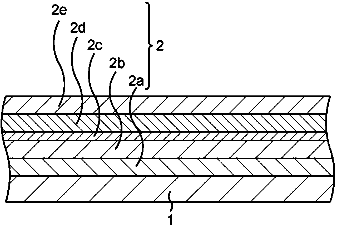
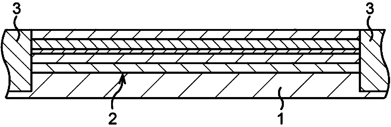
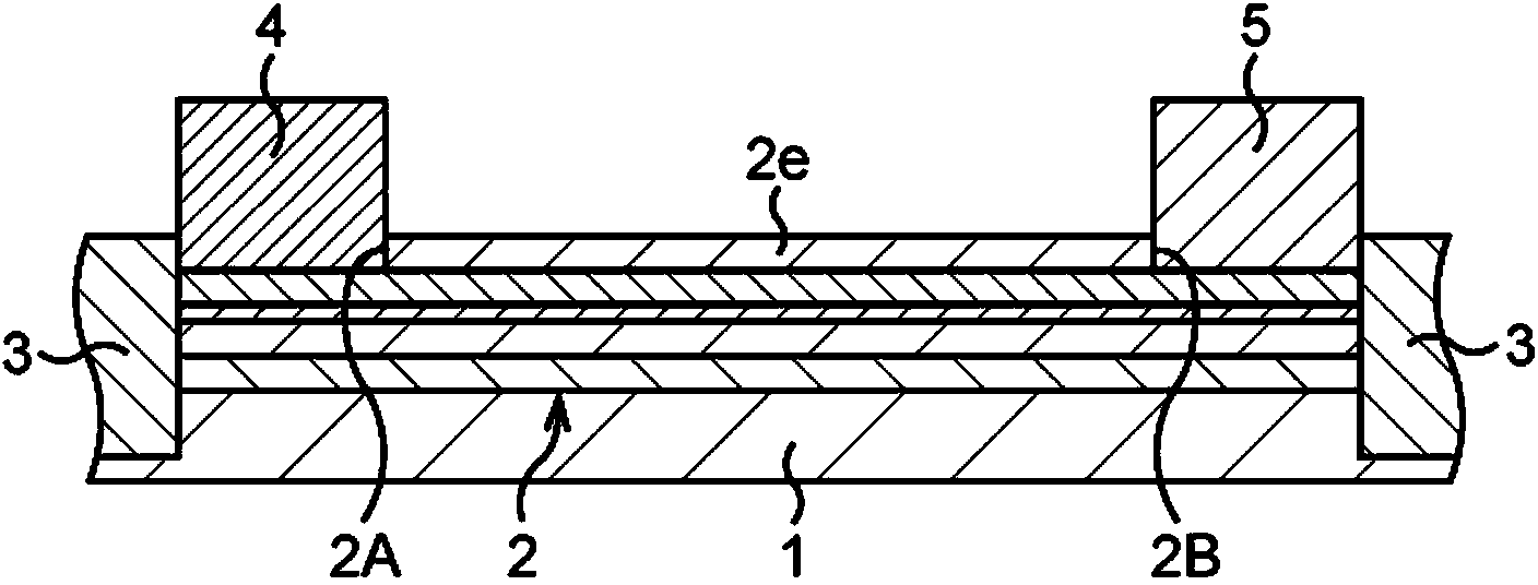
[0035] Figure 1A to Figure 4B is a schematic sectional view illustrating the method of manufacturing the AlGaN / GaN HEMT according to the first embodiment in order of steps.
[0036] First, if Figure 1A As shown, a compound semiconductor stack structure 2 that is a stack of a plurality of compound semiconductor layers is formed on, for example, a semi-insulating SiC substrate 1 that is a growth substrate. A Si substrate, a sapphire substrate, a GaAs substrate, a GaN substrate, or the like may be used instead of the SiC substrate as the growth substrate. The conductivity of the substrate can be semi-insulating or conducting.
[0037] The compound semiconductor stack structure 2 includes a buffer layer 2a, an electron transport layer 2b, a spacer layer 2c, an electron supply layer 2d, and a capping layer 2e.
[0038] In the comp...
Embodiment )
[0103] In the first embodiment and its modified examples, an AlGaN / GaN HEMT is exemplified as a compound semiconductor device. As a compound semiconductor device, the present invention is applicable to the following HEMTs other than AlGaN / GaN HEMTs.
[0104] Other HEMT Examples 1
[0105] In this example, an InAlN / GaN HEMT is disclosed as a compound semiconductor device.
[0106] InAlN and GaN are compound semiconductors whose lattice constants can be made close to each other by composition. In this case, in the above-described first embodiment and its modified examples, the electron transport layer is made of i-GaN, the spacer layer is made of i-AlN, and the electron supply layer is made of n-InAlN, And the cap layer is made of n-GaN. Further, in this case, piezoelectric polarization hardly occurs, and two-dimensional electron gas is thus generated mainly by spontaneous polarization of InAlN.
[0107] According to this example, a highly reliable and high withstand voltage...
no. 2 example )
[0113] In this embodiment, a MOS transistor is disclosed as a semiconductor device.
[0114] Figure 8A to Figure 10B Schematic sectional views of the method of manufacturing a MOS transistor according to the second embodiment are explained in step order.
[0115] First, if Figure 8A As shown, a gate electrode 23 is formed on a Si substrate 21 via a gate insulating film 22 .
[0116] Specifically, element isolation region 20 is formed on Si substrate 21 by, for example, an STI (Shallow Trench Isolation) method. The element isolation region 20 defines an element region on the Si substrate 21 .
[0117] Next, a silicon oxide film is deposited on Si substrate 21 by, for example, a CVD method or the like. Thus, the gate insulating film 22 is formed.
[0118] Then, polysilicon is deposited on the gate insulating film by, for example, a CVD method or the like, and the gate insulating film 22 and the polysilicon are processed into an electrode shape by photolithography and dry ...
PUM
 Abstract
Description
Claims
Application Information