Ceramic insulating film heat-conducting substrate and manufacturing method thereof

A technology of ceramic insulating and thermally conductive substrates, which is used in semiconductor/solid-state device manufacturing, semiconductor devices, and semiconductor/solid-state device components, etc. Realize the effect of industrialization and easy industrialization

Active Publication Date: 2010-12-15
SHENZHEN UNIV
View PDF4 Cites 12 Cited by
  • Summary
  • Abstract
  • Description
  • Claims
  • Application Information

AI Technical Summary

Problems solved by technology

Main problems: 1. The film layer is restricted by the base material and is difficult to control; 2. The process is complicated and takes a long time; 3. The insulating medium layer that does not require the insulating medium layer affects the heat dissipation effect of the substrate; 4. There will be micro-hole conduction , the sealing agent will further reduce the thermal conductivity
[0005] Stainless steel-based metal PCB substrate, the insulating medium layer is a mixture of glass and ceramics, and the metal circuit layer is made of a thick film process; the main problems: 1. Need to use glass as an adhesive, and the thermal conductivity of glass is poor; 2. Available for selection The metal substrate is only stainless steel, and the thermal conductivity of stainless steel is low, which is not conducive to heat dissipation; 3. The sintering process is adopted, the process is complicated, the time is long, and the energy consumption is high
[0006] Epoxy resin packaging method, due to the low thermal conductivity of epoxy resin (0.3W / m·K), the overall heat dissipation effect will be seriously affected, reducing the life of the LED

Method used


Image

  • Ceramic insulating film heat-conducting substrate and manufacturing method thereof
  • Ceramic insulating film heat-conducting substrate and manufacturing method thereof
  • Ceramic insulating film heat-conducting substrate and manufacturing method thereof

Examples


Embodiment Construction

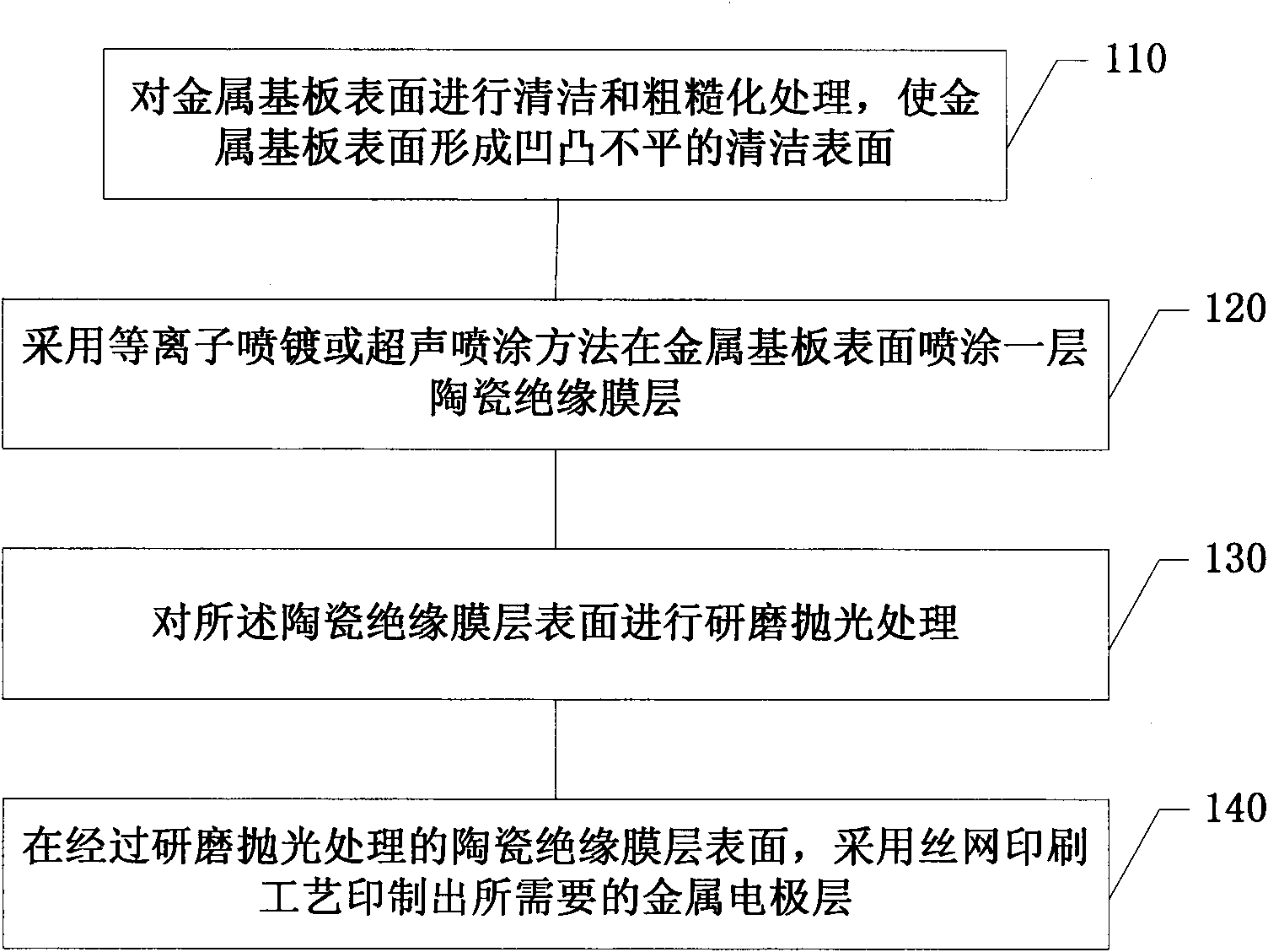
[0037] In order to make the purpose, technical solution and advantages of the present invention clearer and clearer about a ceramic insulating film heat-conducting substrate and its manufacturing method, the present invention will be described in detail below with reference to the accompanying drawings and examples. It should be understood that the specific embodiments described here are only used to explain the present invention, not to limit the present invention.

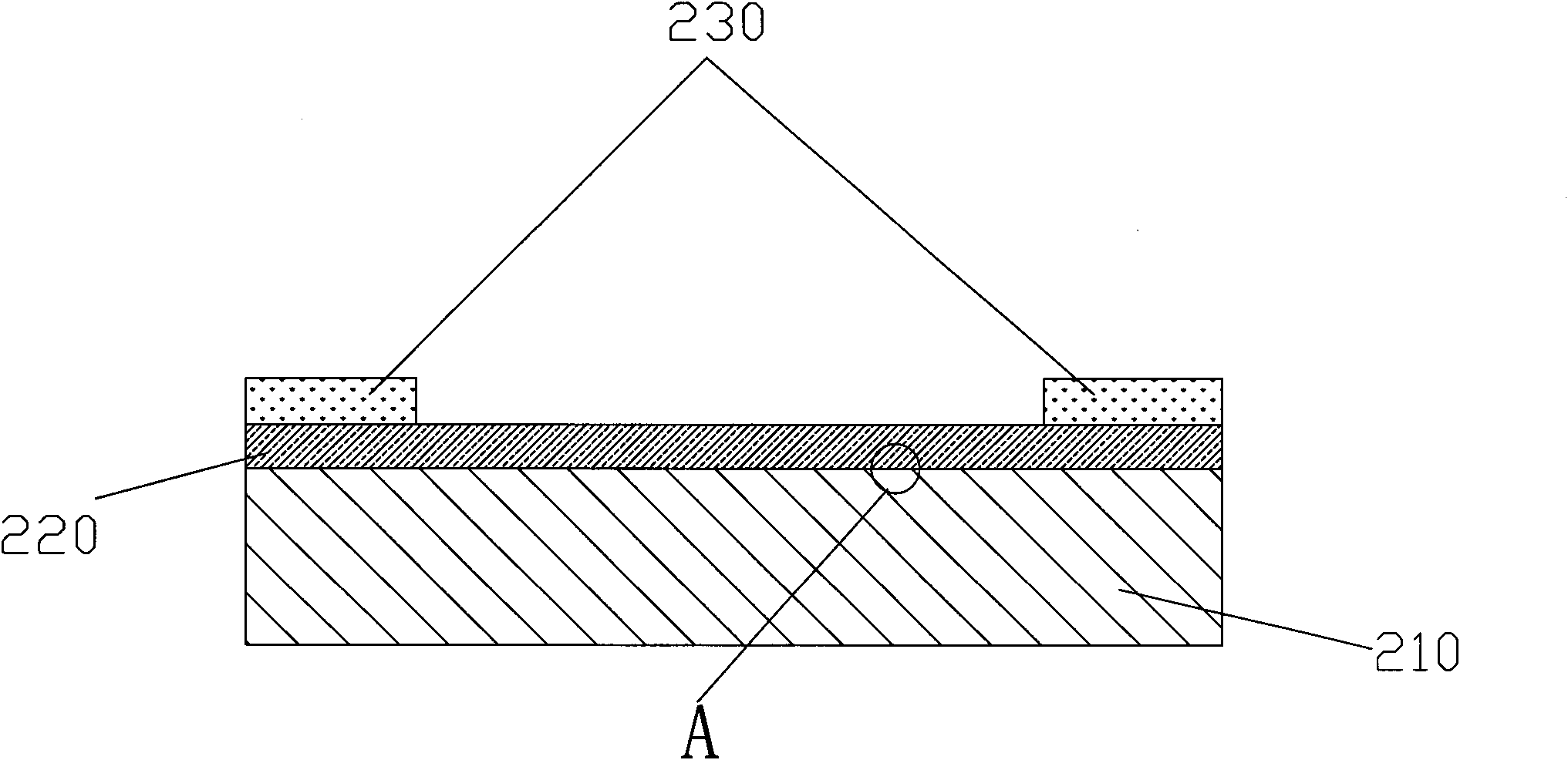
[0038] A kind of manufacture method of ceramic insulation film thermal conduction substrate of the present invention, such as figure 1 shown, including the following steps:

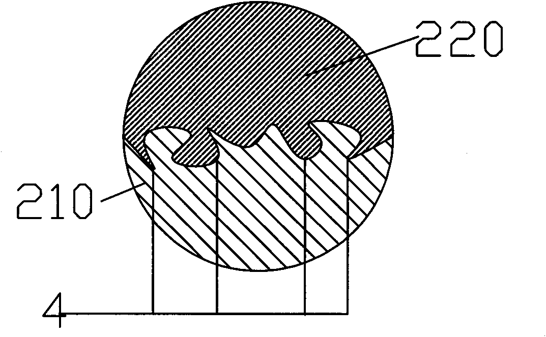
[0039] Step S110, cleaning and roughening the surface of the metal substrate to form a rough and clean surface on the surface of the metal substrate; wherein, the metal substrate is made of one of aluminum, copper, steel, titanium, molybdenum, and tungsten or its alloys, stainless steel, or, Kovar. The surface of the metal substrate can be...


PUM

PropertyMeasurementUnit
thicknessaaaaaaaaaa
thicknessaaaaaaaaaa
thermal conductivityaaaaaaaaaa

Abstract

The invention relates to the technical fields of electronics and photoelectronic packaging, and discloses a ceramic insulating film heat-conducting substrate and a manufacturing method thereof. The surface of a metal substrate is cleaned and roughened, so the surface of the metal substrate becomes a concave-convex clean surface; a layer of ceramic insulating film is sprayed on the surface of the metal substrate by a plasma spraying or ultrasonic spraying method; and a metal electrode layer required is printed on the polished surface of the ceramic insulating film by a screen printing process. The method has the advantages of simple process, low manufacturing cost, good radiating effect and no micropore conduction.

Description

technical field [0001] The invention relates to the technical field of electronic and optoelectronic packaging, in particular to a ceramic insulating film heat-conducting substrate and a manufacturing method thereof. Background technique [0002] Since the rise of the junction temperature during LED operation will reduce the probability of luminous recombination, the lifespan and output luminous flux will also decrease with the increase of temperature. If the heat generated by the PN junction can be dissipated as soon as possible, it will not only improve the luminous efficiency of the product, but also improve the reliability and life of the product. LED chips also have strict requirements on the matching of the linear expansion coefficient of the substrate material. [0003] At present, the more common ceramic substrates on the market are mostly LTCC (Low Temperature Co-fired Ceramic LTCC) or ceramic heat dissipation substrates made of thick film technology. Due to the dif...

Claims


Application Information

Patent Timeline
Patent Type & Authority Applications(China)
IPC IPC(8): H01L21/48H01L23/498H01L23/34
Inventor 柴广跃雷云飞刘文黄长统王少华刘沛徐光辉
Owner SHENZHEN UNIV
Why Eureka
Try Eureka