Semiconductor shallow trench isolation method

A semiconductor and shallow trench technology, applied in semiconductor/solid-state device manufacturing, electrical components, circuits, etc., can solve problems such as corner damage in the active area, device failure, and stress effects in the active area, and achieve the goal of reducing the impact Effect

Active Publication Date: 2010-12-29
CSMC TECH FAB2 CO LTD
View PDF3 Cites 4 Cited by
  • Summary
  • Abstract
  • Description
  • Claims
  • Application Information

AI Technical Summary

Problems solved by technology

[0006] In the existing STI isolation process, when HDP is deposited, plasma is used to bombard the corners of the active region to prevent HDP from prematurely sealing and causing a void in the center of the trench, but the plasma bombardment will cause Plasma damage caused by the corners of the source region
Moreover, the existing HDP is directly deposited on the liner oxide layer. Although the liner oxide layer has a buffer for HDP, HDP still has a stress effect on the active region.
In addition, in the STI process of the prior art, the boron in the active region will accumulate at the junction

Method used


Image

  • Semiconductor shallow trench isolation method
  • Semiconductor shallow trench isolation method
  • Semiconductor shallow trench isolation method

Examples


Embodiment Construction

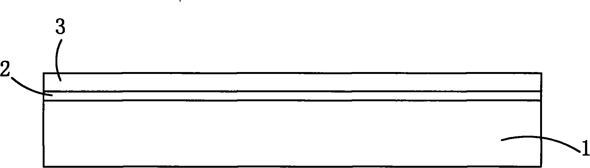
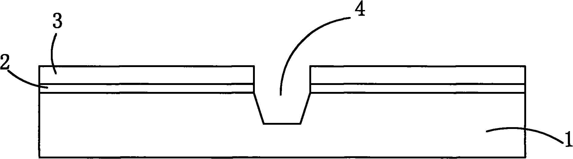
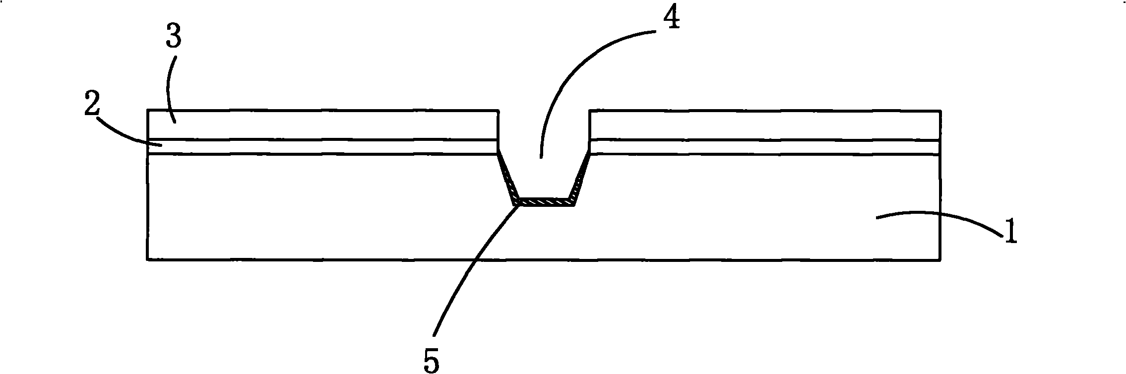
[0015] Those who are familiar with the field of semiconductor manufacturing process should know that in the manufacturing process of a semiconductor chip, it usually goes through many repeated steps of masking, photolithography, etching and ion implantation to form different semiconductor devices and interconnection structures between devices. Wait. The method involved in the present invention is one of the steps in the semiconductor chip manufacturing process, that is, a method for device isolation by using shallow trenches. Therefore, the steps of forming other components in the semiconductor manufacturing process will not be described in detail in this specification.

[0016] In addition, specific and detailed operation methods for various steps in the shallow trench isolation process, such as how to deposit an oxide layer or a silicon nitride layer, or how to etch a silicon oxide layer and a silicon nitride layer, etc. The operation method and other content are the same a...


PUM


Abstract

The invention discloses a device isolation method in semiconductor manufacturing process, including the following steps: a silicon substrate is provided, a pad oxidation layer and a pad silicon nitride layer are deposited on the surface of the silicon substrate; the pad oxidation layer, the pad silicon nitride layer and the silicon substrate are etched, so as to form a trench on the silicon substrate; a lining oxidation layer is formed on the inner wall and bottom surface of the trench; a lining silicon nitride layer is formed on the surface of the lining oxidation layer in the trench; high density plasma chemical vapour deposition method is utilized to deposit a silicon oxide layer on the surface of the silicon substrate; the pad silicon nitride layer and the pad oxidation layer are removed; and etching is carried out on the lining silicon nitride, so that a cavity is formed between an active region and a high density plasma region. The method of the invention can prevent damage of plasma to active region corner as a lining silicon nitride layer is formed on the lining oxidation layer, boron aggregation can be avoided, short corner can be avoided, and stress of high density plasma to the silicon substrate can be reduced.

Description

【Technical field】 [0001] The invention relates to a semiconductor manufacturing method, in particular to a device isolation method using shallow trenches in the semiconductor manufacturing process. 【Background technique】 [0002] An integrated circuit chip usually includes a semiconductor substrate, various semiconductor devices formed by doping different ions into the semiconductor substrate, and an interconnection structure that electrically connects these semiconductor devices to each other to form electrical devices and circuits. [0003] The semiconductor devices formed in the semiconductor chip usually include different devices such as resistors, capacitors, and transistors. One such complementary metal-oxide-semiconductor device (CMOS device) may typically contain N-channel and P-channel metal-oxide-semiconductor field-effect transistors (MOSFETs) formed in oppositely doped adjacent wells, with each field An effect transistor generally includes a source region and a ...

Claims


Application Information

Patent Timeline
IPC IPC(8): H01L21/76H01L21/764H01L21/762H01L21/822H01L21/8238
Inventor 马擎天许宗能朱旋肖玉洁
Owner CSMC TECH FAB2 CO LTD
Why Eureka
Try Eureka