Leadless ceramic chip type gas sensor

A technology of gas sensor and ceramic chip, which is applied in the field of gas sensor, can solve the problems of restricting the expansion and development of the industrial scale of gas sensor production, large dispersion of component performance parameters, limiting development and use direction, etc., and achieving high efficiency Automated production, outstanding practicability, and the effect of solving poor seismic performance

Active Publication Date: 2011-02-16
郑州炜盛电子科技有限公司
View PDF5 Cites 2 Cited by
  • Summary
  • Abstract
  • Description
  • Claims
  • Application Information

AI Technical Summary

Problems solved by technology

[0002] At present, the structure of the side-heated metal oxide semiconductor gas sensor in China is mainly a suspended structure, and the anti-seismic performance of the suspended structural element is poor. The characteristics lead to large dispersion of performance parameters of such components and high production costs. At the same time, it greatly limits the expansion and development of the industrial scale of production of such gas sensors.
[0003] The existing chip-type thick-film semiconductor gas-sensing element gas-sensing chip uses a thick-film screen printing process to manufacture heaters and gas-sensing materials on both sides of the ceramic substrate. In the metal casing, the salt spray corrosion resistance of this type of gas sensor is poor. At the same time, the lack of this type of gas sensor also limits its development and application direction

Method used


Image

  • Leadless ceramic chip type gas sensor
  • Leadless ceramic chip type gas sensor
  • Leadless ceramic chip type gas sensor

Examples


Embodiment Construction

[0017] The technical solutions of the present invention will be described in further detail below through specific implementation methods.

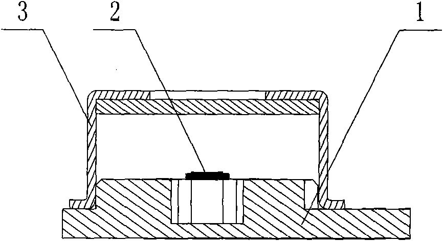
[0018] Such as figure 1 As shown, a leadless ceramic chip gas sensor, it includes a ceramic base 1, a ceramic chip gas sensor chip 2 and a metal shell 3, the ceramic base 1 and the ceramic chip gas sensor chip 2 Encapsulated in the metal case 3;

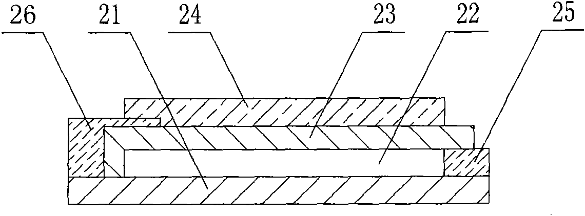
[0019] Such as figure 2 As shown, the ceramic chip gas sensor chip 2 includes a ceramic substrate 21, a heating resistor 22, a heating electrode 25 connected to the heating resistor 22, an isolation layer 23, a gas sensitive material 24 and a measuring electrode 26 connected to the gas sensitive material 24 , wherein one side of the ceramic substrate 21 and one side of the heating resistor 22 are printed together using thick film screen printing technology, and the other side of the heating resistor 22 and the side of the isolation layer 23 are printed using thick film silk Printed together ...


PUM


Abstract

The invention provides a leadless ceramic chip type gas sensor which comprises a ceramic base and a ceramic chip type gas sensitive chip; the gas sensing chip comprises a ceramic substrate, a heating resistor, a heating electrode, an isolation layer, a gas sensing material and a measuring electrode, wherein the ceramic substrate, the heating resistor, the isolation layer and the gas sensing material are sequentially printed together; a through hole and a printing electrode penetrating the through hole are arranged on the ceramic base, a heating electrode printing point and a measuring electrode printing point are arranged on the front surface of the ceramic base, an heating electrode input end and a measuring electrode output end are arranged on the back surface of the ceramic base, and the heating electrode printing point and the measuring electrode printing point are respectively connected with the heating electrode input end and the measuring electrode output end through the printing electrode; and the heating electrode and the measuring electrode are respectively connected on the heating electrode printing point and the measuring electrode printing point. The gas sensor has the advantages of scientific design, stable performance running, high sensitivity and high precision, and is applicable to industrial large-scale production.

Description

technical field [0001] The invention relates to a gas sensor, in particular to a leadless ceramic chip gas sensor. Background technique [0002] At present, the structure of the side-heated metal oxide semiconductor gas sensor in China is mainly a suspended structure, and the anti-seismic performance of the suspended structural element is poor. The characteristics lead to large dispersion of performance parameters of such components and high production costs. At the same time, it greatly limits the expansion and development of the industrial scale of production of such gas sensor components. [0003] The existing chip-type thick-film semiconductor gas-sensing element gas-sensing chip uses a thick-film screen printing process to manufacture heaters and gas-sensing materials on both sides of the ceramic substrate. In the metal casing, the salt spray corrosion resistance of this type of gas sensor is poor. At the same time, the shortage of this type of gas sensor also limits i...

Claims


Application Information

Patent Timeline
Patent Type & Authority Applications(China)
IPC IPC(8): G01N27/00
Inventor 张小水钟克创张开文祁明锋王利利
Owner 郑州炜盛电子科技有限公司
Why Eureka
Try Eureka