Laminated electronic component and method for manufacturing the same

Active Publication Date: 2009-11-26
MURATA MFG CO LTD
View PDF23 Cites 23 Cited by
  • Summary
  • Abstract
  • Description
  • Claims
  • Application Information

AI Technical Summary

Benefits of technology

[0010]To overcome the problems described above, preferred embodiments of the present invention provide a laminated electronic component including external terminal electr

Problems solved by technology

However, there is a problem in that as the thickness of the ceramic layer is reduced, short-circuiting between internal electrodes readily occurs and, thereby, it is difficult to ensure quality.
However, in mass production of the laminated ceramic capacitor, it is necessary to provide a side margin between an internal electrode and a side surface of a ceramic element assembly and an end margin between the internal electrode and the end surface of the ceramic element assembly due to deviations in lamination and deviations in cutting of the ceramic green sheets.
However, there is a limit to the amount of increase in the area of the ceramic layer within the bounds of a dimensional

Method used


Image

  • Laminated electronic component and method for manufacturing the same
  • Laminated electronic component and method for manufacturing the same
  • Laminated electronic component and method for manufacturing the same

Examples


first preferred embodiment

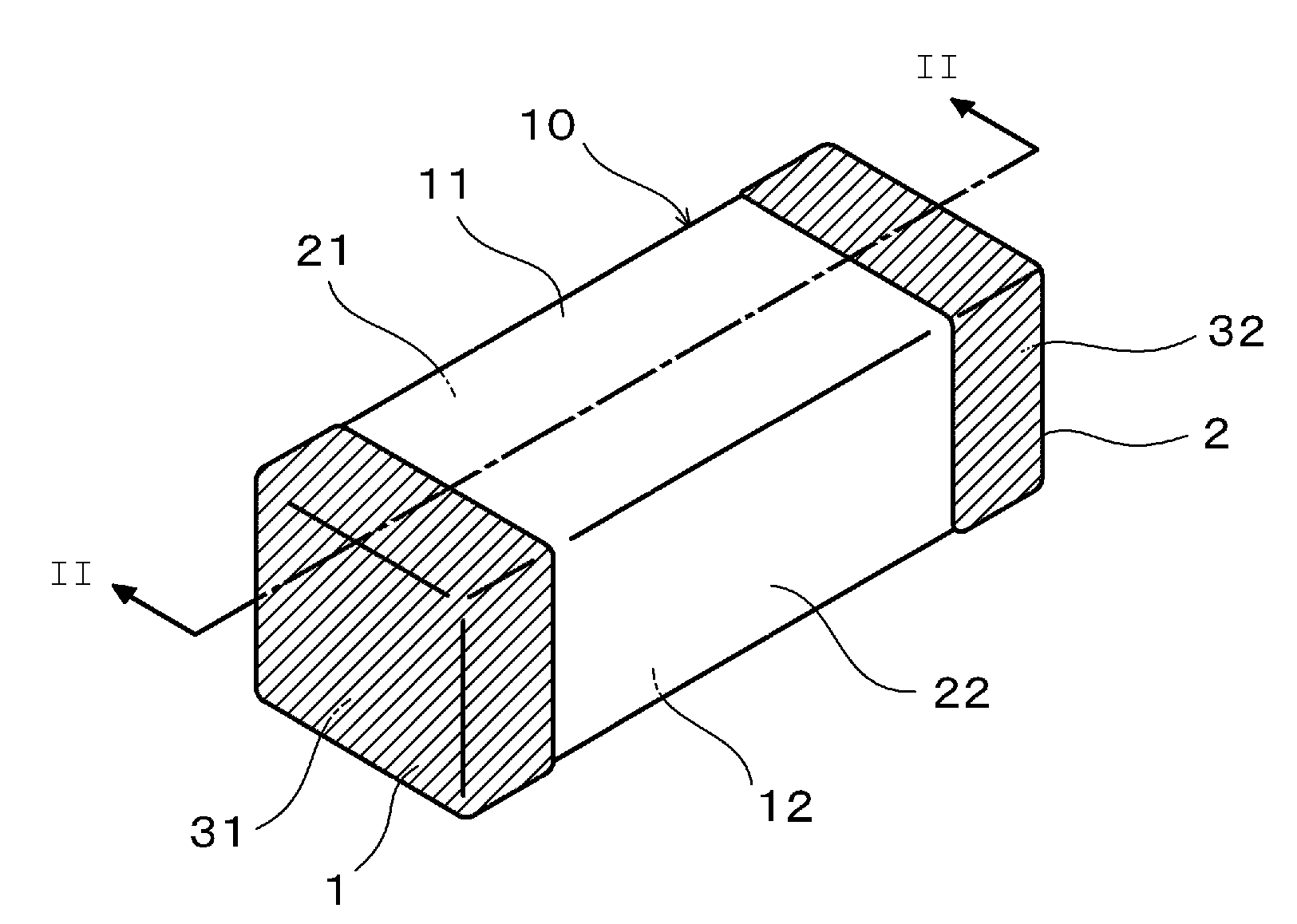
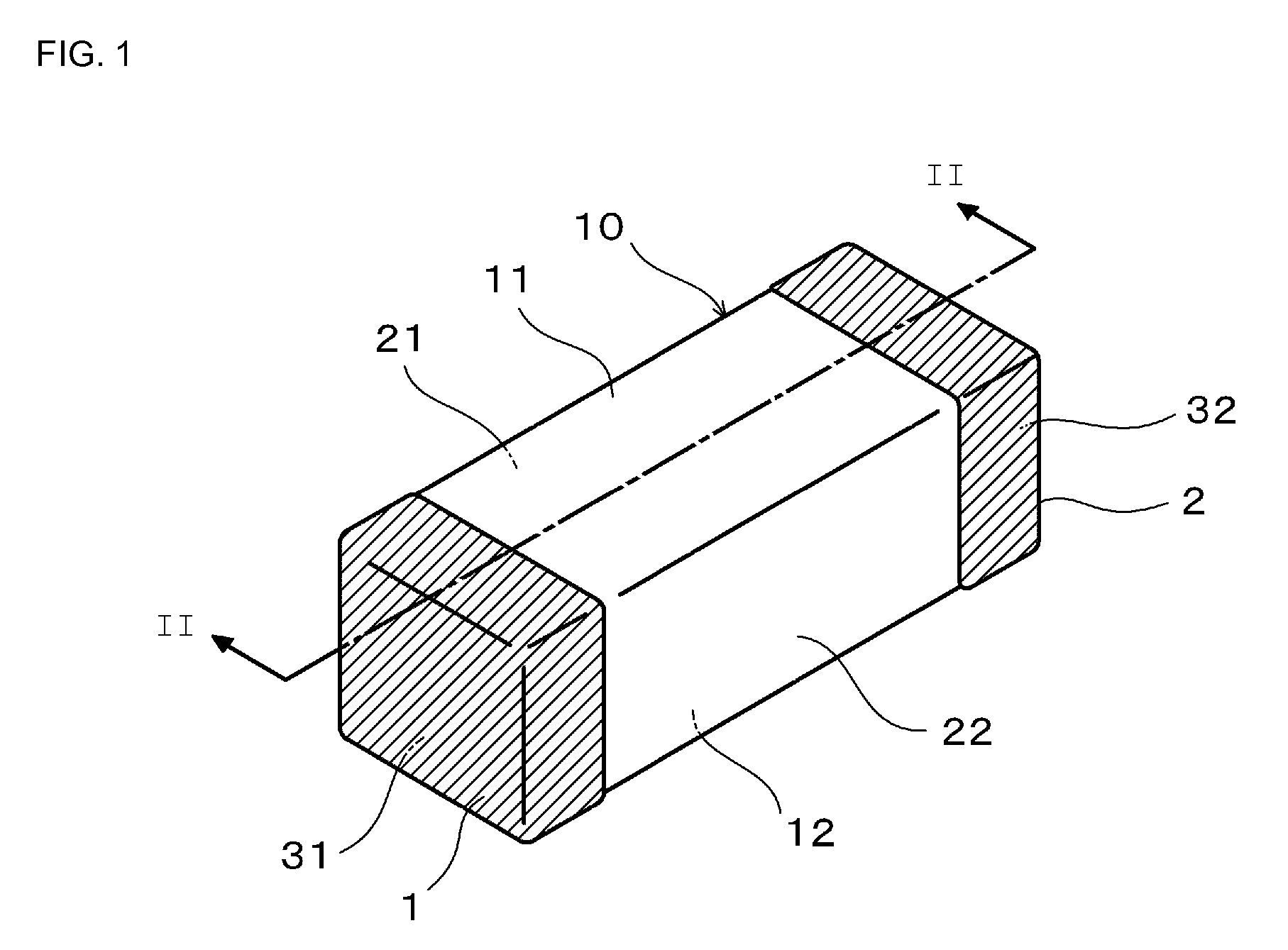
[0033]In the first preferred embodiment of the present invention, a two-terminal type laminated ceramic capacitor including a pair of external terminal electrodes defined by one Cu plating film layer will be described as an example of a laminated electronic component.

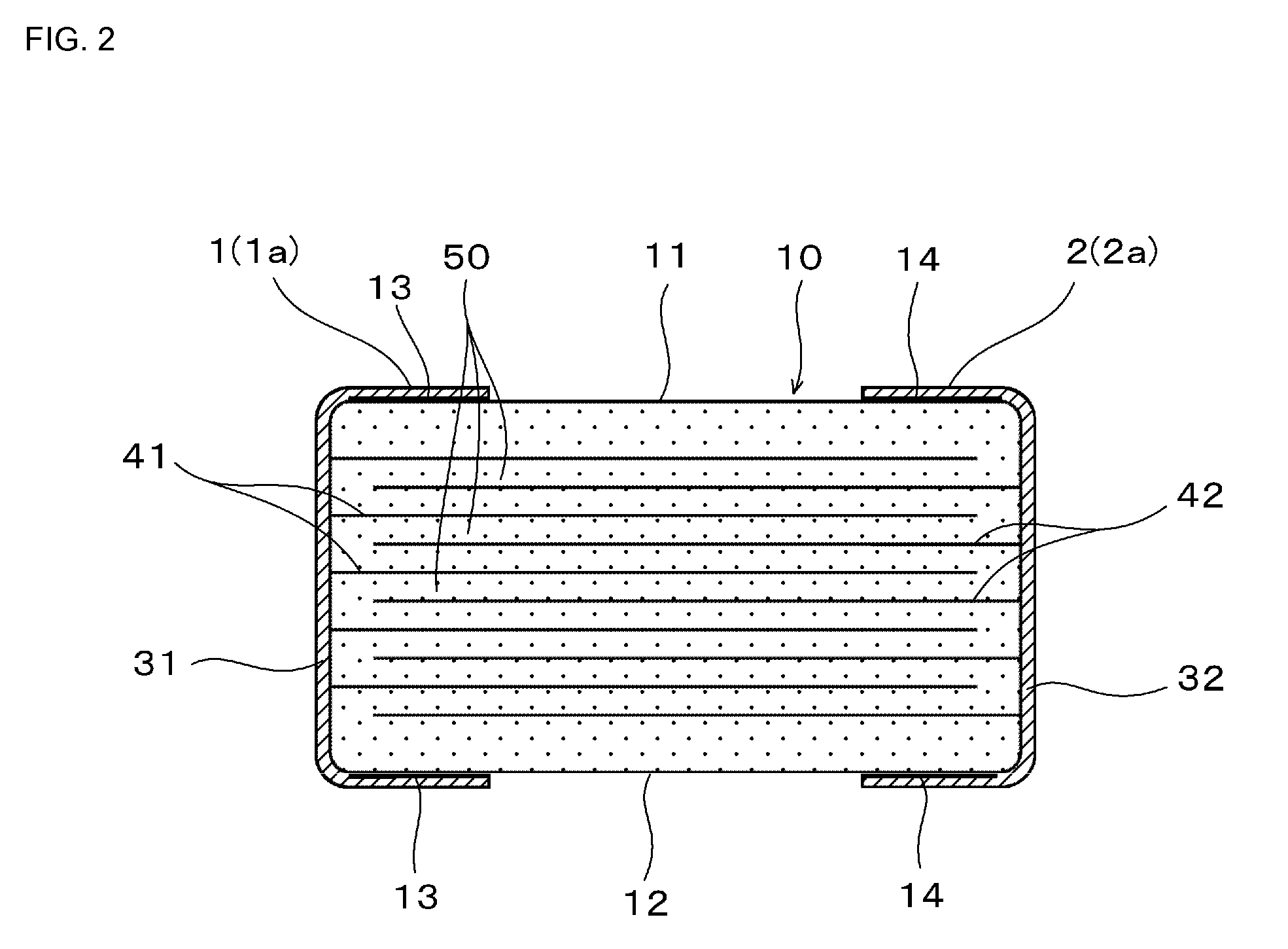
[0034]FIG. 1 is a perspective view showing an external configuration of a laminated ceramic capacitor according to the first preferred embodiment of the present invention. FIG. 2 is a sectional view of a section taken along a line II-II shown in FIG. 1. FIG. 3 is a diagram showing internal electrode patterns of this laminated ceramic capacitor. FIG. 4 is a diagram showing a magnified portion, e.g., a connection portion between an external terminal electrode and an internal electrode.

[0035]The laminated ceramic capacitor includes a capacitor main body 10 in the shape of a substantially rectangular parallelepiped having a first principal surface 11 and a second principal surface 12 that are opposite to each other, a first...

second preferred embodiment

[0076]FIG. 5 is a diagram showing a magnified portion of a laminated ceramic capacitor according to a second preferred embodiment of the present invention. The configurations and materials of the laminated ceramic capacitor according to the second preferred embodiment are substantially the same as those in the laminated ceramic capacitor according to the first preferred embodiment except that the first (and the second) external terminal electrode 1 (2) includes only the substrate plating film 1a (2a).

[0077]FIG. 5 shows a connection portion between the first external terminal electrode 1 disposed on the first end surface 31 of the capacitor main body 10 and the first internal electrode 41. On the other hand, a connection portion between the second external terminal electrode 2 (refer to FIGS. 1 and 2) and the second internal electrodes 42 and the connection portion shown in FIG. 5 are mirror images of each other. Therefore, the substrate plating film 2a and the second internal electr...

third preferred embodiment

[0080]FIG. 6 is a diagram showing a laminated ceramic capacitor according to a third preferred embodiment of the present invention. The laminated ceramic capacitor according to the third preferred embodiment has substantially the same configuration as that of the laminated ceramic capacitor according to the first embodiment except that the capacitor main body 10 includes dummy internal electrodes D (D1, D2). In FIG. 6, the same portions as or the portions corresponding to those shown in FIG. 2 are indicated by the same reference numerals as those set forth above.

[0081]For dummy electrodes D in the laminated ceramic capacitor, first dummy internal electrodes D1 that extend to the first end surface 31 and second dummy internal electrodes D2 that extend to the second end surface 32 are provided. The first dummy electrodes D1 and the second dummy electrodes D2 are disposed on the same or substantially the same planes as those on which the individual internal electrodes 41 and 42 between...


PUM

PropertyMeasurementUnit
Particle diameteraaaaaaaaaa

Abstract

A laminated electronic component is configured to include substrate plating films disposed on outer surfaces of an electronic component main body through direct plating such that external terminal electrodes are connected to exposed portions of internal conductors (internal electrodes), and the average particle diameter of metal particles defining the substrate plating film is at least about 1.0 μm. The external terminal electrode includes at least one layer of an upper plating film disposed on the substrate plating film. The metal particles defining the substrate plating film are Cu particles.

Description

BACKGROUND OF THE INVENTION[0001]1. Field of the Invention[0002]The present invention relates to a laminated electronic component and a method for manufacturing the same. In particular, the present invention relates to a laminated electronic component in which external terminal electrodes connected to internal conductors are formed on outer surfaces of an electronic component main body through a direct plating step and a method for manufacturing the same.[0003]2. Description of the Related Art[0004]In recent years, the market for small portable electronic equipment, e.g., cellular phones, notebook personal computers, digital cameras, and digital audio equipment, has been increasing. In the portable electronic equipment, miniaturization has been advanced which, at the same time, performance has been improved. A plurality of laminated electronic components are mounted on the portable electronic equipment, and miniaturization and performance enhancement of these laminated electronic co...

Claims


Application Information

Patent Timeline
IPC IPC(8): H01G4/005B05D5/12
CPCH01G4/005H01G4/008Y10T29/417Y10T29/435Y10T29/43H01G4/2325
Inventor TAKEUCHI, SHUNSUKEKAWASAKI, KENICHIMOTOKI, AKIHIROOGAWA, MAKOTOIWANAGA, TOSHIYUKI
Owner MURATA MFG CO LTD
Why Eureka
Try Eureka