Display
A display and display area technology, applied in instruments, identification devices, printing devices, etc., can solve problems such as difficulty in setting
- Summary
- Abstract
- Description
- Claims
- Application Information
AI Technical Summary
Problems solved by technology
Method used
Image
Examples
Embodiment Construction
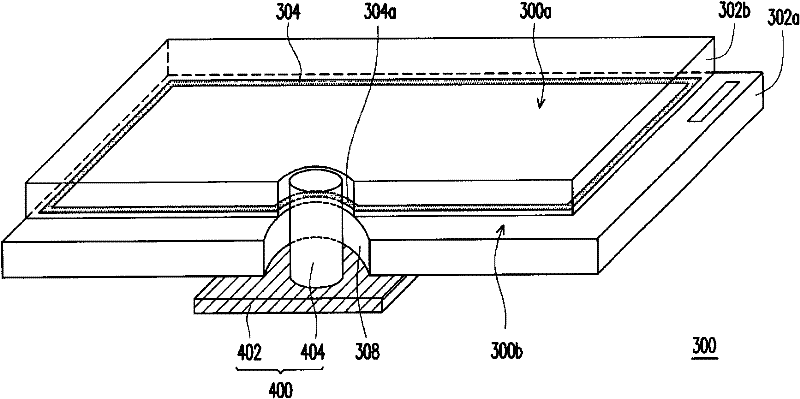
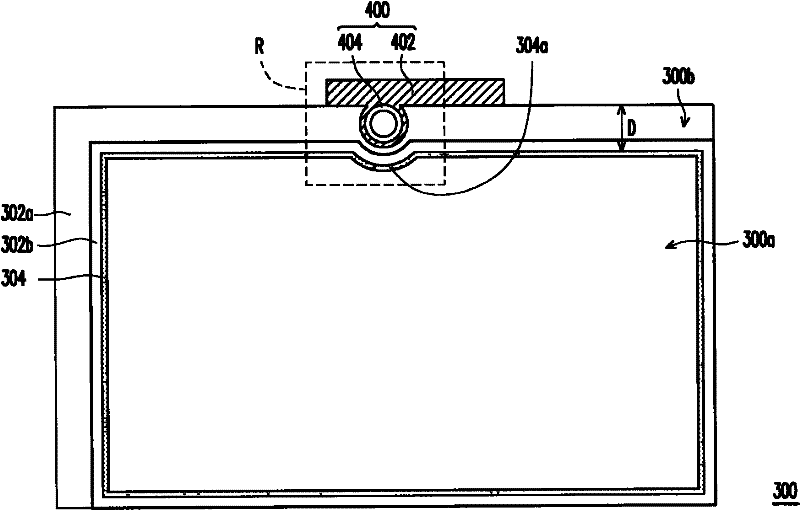
[0041] Figure 2A It is a three-dimensional schematic diagram of a display according to an embodiment of the present invention. Figure 2B for Figure 2A top view diagram. and image 3 , Figure 4A to Figure 4J as well as Figure 5 for Figure 2B An enlarged schematic view of the local region R of .
[0042] Please refer to Figure 2A The display in this embodiment includes a display panel 300 and an image capture device 400, wherein the display panel 300 includes a first substrate 302a, a second substrate 302b, a sealant 304, and a display medium (not shown).
[0043] In this embodiment, the first substrate 302a is, for example, an active device array substrate. Specifically, the first substrate 302a is, for example, a thin film transistor array substrate, and the thin film transistor array substrate has a plurality of scanning lines (not shown), a plurality of data lines (not shown), a plurality of thin film transistors (not shown). shown) and a plurality of pixel u...
PUM
 Abstract
Description
Claims
Application Information


