Adhesive sheet for supporting and protecting semiconductor wafer, back grinding method for semiconductor wafer

A technology of semiconductors and adhesive sheets, which is applied in the direction of semiconductor devices, semiconductor/solid-state device manufacturing, adhesive types, etc., can solve the problems of residual glue, insufficient follow-up of sheets, processing errors, etc., and achieve the goal of preventing glue residue Effect

Inactive Publication Date: 2011-03-30
NITTO DENKO CORP
View PDF2 Cites 8 Cited by
  • Summary
  • Abstract
  • Description
  • Claims
  • Application Information

AI Technical Summary

Problems solved by technology

[0007] Therefore, in the method of using the conventional adhesive sheet, the sheet cannot sufficiently follow the unevenness, and the bonding between the adhesive and the wafer surface is insufficient.
As a result, during wafer processing, peeling of flakes, intrusion of grinding water and foreign matter into the pattern surface, processing errors, dents, chip flying, etc. may occur, and wafer damage may occur.
[0008] In addition, when the adhesive sheet is peeled off from the semiconductor wafer, the adhesive embedded in the unevenness may be broken, and adhesive residue may be generated on the semiconductor wafer side.
In particular, when a relatively soft adhesive is used in order to make the adhesive sheet follow unevenness well, there is a problem that more adhesive residue occurs

Method used


Image

  • Adhesive sheet for supporting and protecting semiconductor wafer, back grinding method for semiconductor wafer
  • Adhesive sheet for supporting and protecting semiconductor wafer, back grinding method for semiconductor wafer
  • Adhesive sheet for supporting and protecting semiconductor wafer, back grinding method for semiconductor wafer

Examples


Embodiment 1

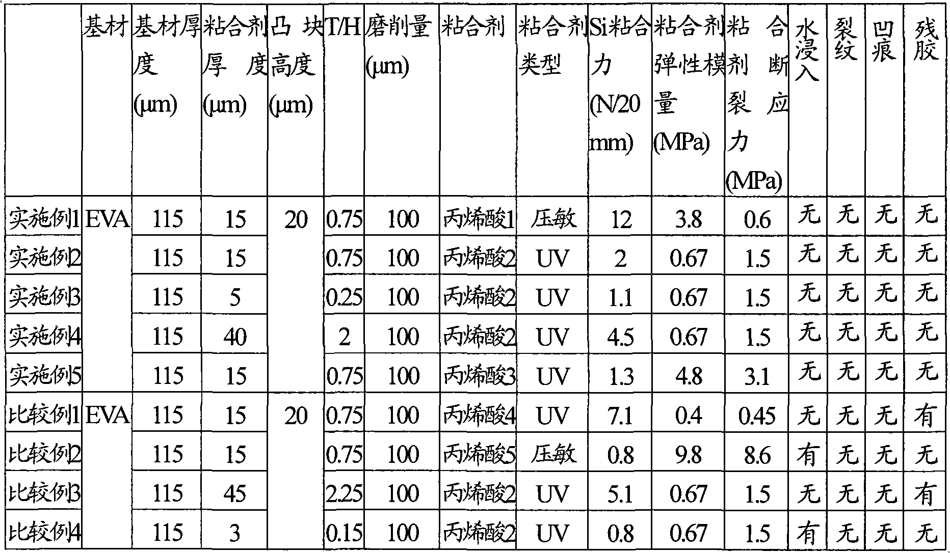
[0161] As the substrate layer, an ethylene-vinyl acetate copolymer (EVA) film with a thickness of 115 μm was used.

[0162] A pressure-sensitive adhesive layer (thickness: 15 μm) was formed thereon.

[0163] For the pressure-sensitive adhesive layer, the adhesive solution of the above-mentioned acrylic adhesive 1 was applied to a silicone release-treated polyester film with a thickness of 38 μm to a thickness of 50 μm after drying, and dried at 120°C 2 minutes.

[0164] Thereafter, a 115 μm EVA film was laminated as a base material to prepare an adhesive sheet for holding and protecting a semiconductor wafer.

[0165] The obtained adhesive sheet for holding and protecting the semiconductor wafer was heated at 50° C. and aged for 1 day or more to obtain an adhesive sheet.

[0166] When the adhesive force of the obtained adhesive sheet to the silicon wafer was measured, it was 12 N / 20 mm.

Embodiment 2~5 and comparative example 1~4

[0168] As the substrate layer, an ethylene-vinyl acetate copolymer (EVA) film having a thickness of 115 μm was used in the same manner as in Example 1.

[0169] Using the adhesives shown in Table 1, according to Example 1, an adhesive layer was formed on the substrate layer with the thickness in Table 1.

[0170] The adhesive strengths of the obtained adhesive sheets to silicon wafers were measured, respectively. The results are shown in Table 1.

[0171] Each of the obtained adhesive sheets was adhered to a silicon wafer, ground, peeled off the adhesive sheet, "water immersion", "wafer crack after grinding", "wafer dent" and " Wafer Contamination” evaluation. Moreover, 25 adhesive sheets of each Example and a comparative example were prepared and evaluated. The results are shown in Table 1.

[0172] paste

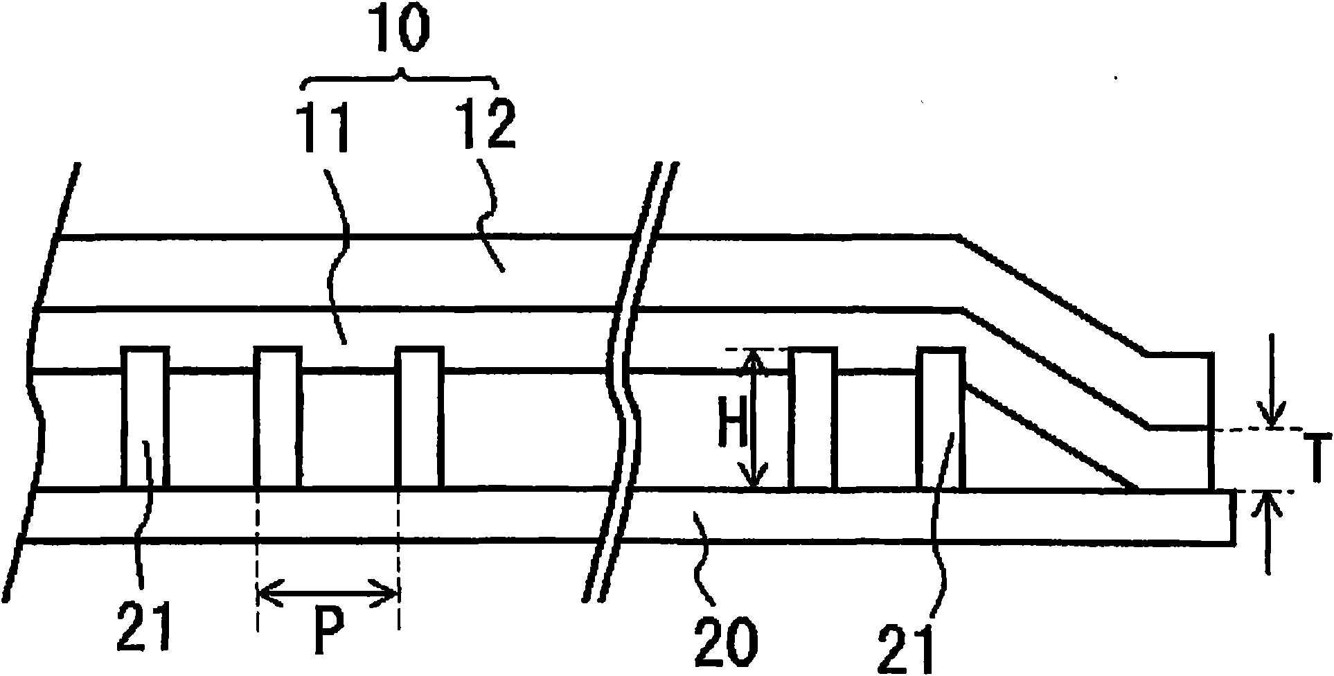
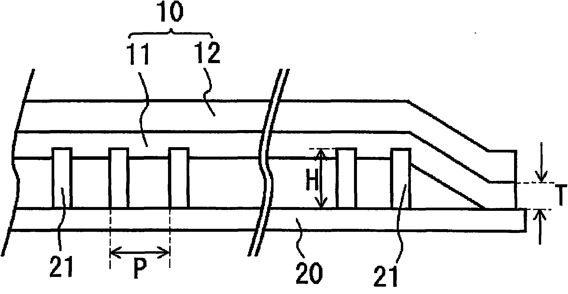
[0173] Each adhesive sheet was pasted so that the adhesive layer 11 was disposed on the surface side of the 6-inch silicon wafer 20 on which the bump electrode 21 w...


PUM

PropertyMeasurementUnit
thicknessaaaaaaaaaa
elastic modulusaaaaaaaaaa
thicknessaaaaaaaaaa

Abstract

The invention aims at providing an adhesive sheet for supporting and protecting a semiconductor wafer, and a back grinding method for the semiconductor wafer. The adhesive sheet can effectively prevent adhesive residue caused by concave-convex parts in a forming surface of circuit patterns and the like of the semiconductor wafer in recent years. The adhesive sheet for supporting and protecting the semiconductor wafer (10) is used for being adhered to a surface of a semiconductor wafer (20) to support and protect the semiconductor wafer (20), a single surface of a substrate layer (12) is provided with an adhesive layer (11), the adhesive layer (11) has a thickness of 4 to 42 mum and an elastic modulus at 25 DEG C of 0.5 to 9 MPa.

Description

technical field [0001] The present invention relates to an adhesive sheet for holding and protecting a semiconductor wafer and a backside grinding method for a semiconductor wafer. And back grinding method of semiconductor wafer. Background technique [0002] In the back grinding process of grinding the back surface of the semiconductor wafer and the dicing process of cutting the wafer into individual chips (chips), damage to the pattern surface, grinding debris, and grinding water may occur. pollution etc. [0003] In addition, since the semiconductor wafer itself is thin and brittle, and the patterned surface of the semiconductor wafer has uneven electrodes and the like, there is a problem that even a small external force is likely to cause damage. [0004] In order to protect the circuit pattern formation surface of this semiconductor wafer during processing and to prevent contamination, damage, etc. of the semiconductor wafer, a method of pasting an adhesive sheet such...

Claims


Application Information

Patent Timeline
Patent Type & Authority Applications(China)
IPC IPC(8): C09J7/02C09J133/08C09J4/06C09J4/02H01L21/68H01L21/304
CPCH01L21/6836C09J2201/622C09J7/0217H01L2221/6834C09J2203/326C09J7/385C09J2301/312Y10T428/264
Inventor 佐佐木贵俊浅井文辉水野浩二
Owner NITTO DENKO CORP
Why Eureka
Try Eureka