Semiconductor structure and fabrication method thereof

A manufacturing method and semiconductor technology, applied in the fields of semiconductor/solid-state device manufacturing, semiconductor devices, transistors, etc., can solve the problems of affecting the feature size of semiconductor structures, affecting the quality and performance of SRAM, and unstable LDD feature size, and achieving good product quality. and performance, short process cycle and good activity effect

Active Publication Date: 2021-06-25
SEMICON MFG INT (SHANGHAI) CORP +1
View PDF0 Cites 0 Cited by
  • Summary
  • Abstract
  • Description
  • Claims
  • Application Information

AI Technical Summary

Problems solved by technology

[0003] However, in the photolithography process, photoresist residue often occurs, and the remaining photoresist will affect the critical dimension (CD) of the semiconductor structure.
For example: in the photolithography process of the Lightly Doped Drain (LDD) of the static random access memory unit (SRAMCell), there will be N-H bond reaction to form residual glue (Scum), in which the N bond comes from the polysilicon sidewall The silicon nitride sidewall, the H bond comes from the air or the cleaning process, and the residual glue will volatilize and decrease with time, causing the characteristic size (CD) of the LDD to be unstable, thus affecting the quality and performance of the SRAM

Method used


Image

  • Semiconductor structure and fabrication method thereof
  • Semiconductor structure and fabrication method thereof
  • Semiconductor structure and fabrication method thereof

Examples


Embodiment Construction

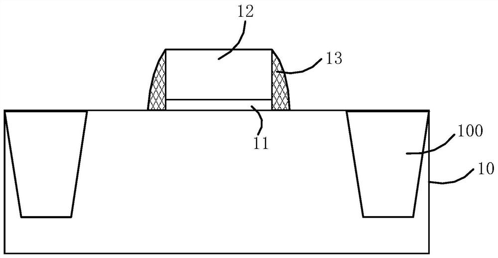
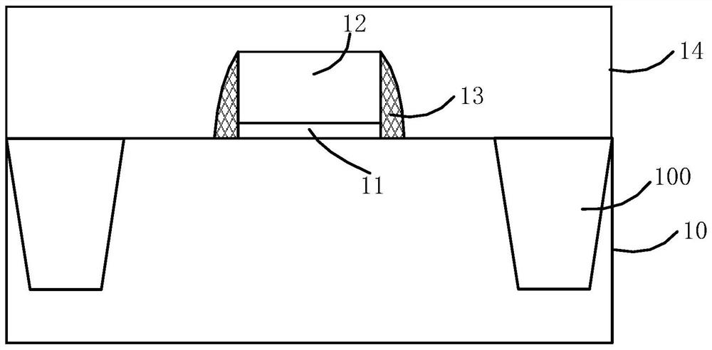
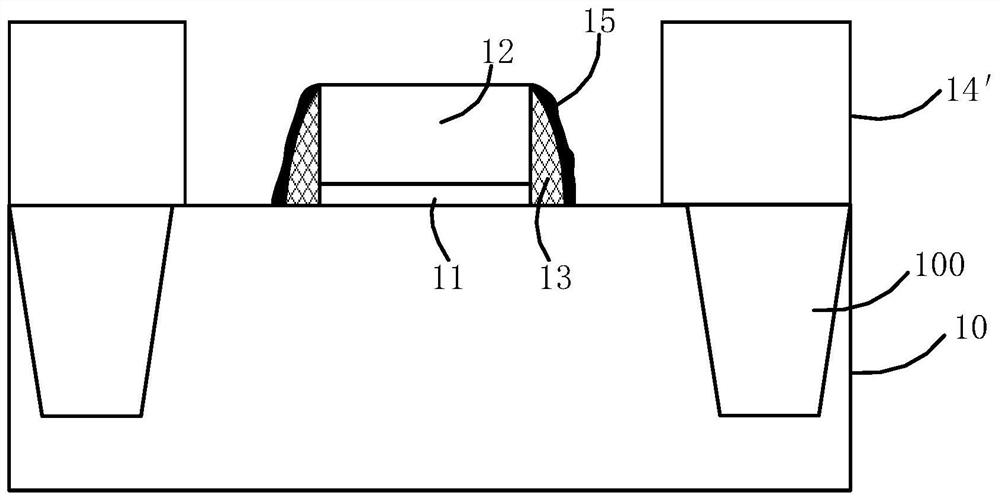
[0028] see Figure 1 to Figure 5 , showing a structural diagram corresponding to each step in a method for manufacturing a semiconductor structure. The method for manufacturing a semiconductor structure includes: providing a first substrate 10 in which a first isolation structure 100 is defined. and an active region (the schematic diagram is omitted in the figure); a first gate structure 12 is formed on the first substrate 10, and the first gate structure 12 covers part of the first substrate 10, usually, in the A first dielectric layer 11 is also included between the first substrate 10 and the first gate structure 12, and the first dielectric layer 11 may be a tunnel oxide layer or a mixture of a high-K insulating layer and a metal layer. layer, the material of the first gate structure 12 may be polysilicon; a first sidewall 13 is formed on the two side walls of the first gate structure 12, and the material of the first sidewall 13 is silicon nitride ,like figure 1 shown. ...


PUM


Abstract

The invention discloses a semiconductor structure and a manufacturing method thereof. The manufacturing method comprises: forming a nitrogen-containing compound layer on a substrate; performing a heat treatment process on the nitrogen-containing compound layer; forming a photoresist pattern layer, and the photoresist pattern layer exposing at least part of the nitrogen-containing compound layer. In the present invention, before forming a photoresist pattern layer, a heat treatment process is performed on the nitrogen-containing compound layer, the heat treatment process can destroy the activity of nitrogen bonds on the surface of the nitrogen-containing compound layer, so that during the formation of the photoresist pattern layer, the nitrogen-containing compound layer There will be no nitrogen bonds on the surface to react with air or hydrogen bonds in the cleaning process, thereby preventing the generation of adhesive residue. In this way, the CD of the semiconductor structure manufactured by the manufacturing method is stable, and has good product quality and performance.

Description

technical field [0001] The invention relates to the field of semiconductor manufacturing, in particular to a semiconductor structure and a manufacturing method thereof. Background technique [0002] In the field of semiconductor manufacturing, the photolithography process is an extremely critical step in the manufacturing method of semiconductor structures. Whether it can accurately move the corresponding pattern to the semiconductor substrate is one of the main factors that determine the performance and quality of semiconductor structures. Generally, the photolithography process includes several main steps such as glue coating, exposure, development and glue removal. Nowadays, with the development of continuous reduction in the size of semiconductor structures, the photolithography process will face more severe challenges, which have a key impact on the performance, quality and yield of semiconductor structures. [0003] However, in the photolithography process, photoresis...

Claims


Application Information

Patent Timeline
Patent Type & Authority Patents(China)
IPC IPC(8): H01L21/336H01L29/78H01L29/08H01L21/8244H01L27/11
CPCH01L29/0847H01L29/66492H01L29/7833H10B10/12
Inventor 胡扬汪军
Owner SEMICON MFG INT (SHANGHAI) CORP
Why Eureka
Try Eureka